DEMO908AP64E Freescale Semiconductor, DEMO908AP64E Datasheet - Page 10
DEMO908AP64E
Manufacturer Part Number
DEMO908AP64E
Description
BOARD DEMO FOR 908AP64
Manufacturer
Freescale Semiconductor
Type
MCUr
Datasheet
1.DEMO908AP64E.pdf
(16 pages)
Specifications of DEMO908AP64E
Contents
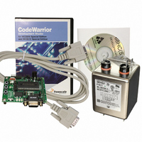
Board, CDs, Cable, Filter
Silicon Manufacturer
Freescale
Core Architecture
HC08
Core Sub-architecture
HC08
Silicon Core Number
MC68HC908
Silicon Family Name
HC08AP
Kit Contents
Board Cables CD Docs
Rohs Compliant
Yes
For Use With/related Products
908AP64
Lead Free Status / RoHS Status
Lead free / RoHS Compliant


D E M O 9 0 8 A P 6 4
Timing
The DEMO908AP64 provides two timing sources. A 9.8304 MHz clock oscillator, at X1, sup-
ports debug monitor operation. A 32.768 kHz crystal oscillator at Y1 provides the base oper-
ating frequency to the MCU for normal operation. The user should refer to the HC08 device
user manual for information on frequency selection. The OSC_SEL jumper selects the timing
input source.
Figure 3: OSC_SEL Jumper Settings
RS-232 Communications
The DEMO908AP64 module provides a single SCI communications port. This port is con-
nected to the MCU_PORT connector and to the COM connector. An RS-232 translator (U3)
provides RS-232 signal level to TTL/CMOS logic level translation on the COM port. Signals
TXD and RXD are routed between the transceiver and the MCU. These signals are also
routed to connector J1. RS-232 communication signals input on J1 must be TTL/CMOS logic
levels; no translation support is provided through this path. The transceiver output may also
be driven off-module if a suitably interface is used. As added development support, hardware
flow control signals RTS and CTS are available on the logic side of U3. These signals are
routed to vias located near the transceiver (U3). RTS has been biased properly to support 2-
wire RS-232 communications.
Use of the J1 connector to input RS-232 signals requires disabling the on-board RS-232 trans-
ceiver to prevent signal corruption. Disabling the on-board transceiver is accomplished by re-
moving the COM_SEL jumper. Details on the COM_SEL jumper are shown in the table below.
Table 2: COM Connections
HC08 Port
PTB2/TXD
PTB3/RXD
1
3 Selects X1 Timing Input – 9.8304 MHz
Selects Y1 Timing Input – 32.768 kHz
COM Signal
TXD OUT
RXD IN
10
Connector
I/O
J1-5
J1-7
PORT
J U N E
2 8 ,
2 0 0 4
Related parts for DEMO908AP64E
Image
Part Number
Description
Manufacturer
Datasheet
Request
R

Part Number:
Description:
Manufacturer:
Freescale Semiconductor, Inc
Datasheet:
Part Number:
Description:
Manufacturer:
Freescale Semiconductor, Inc
Datasheet:
Part Number:
Description:
Manufacturer:
Freescale Semiconductor, Inc
Datasheet:
Part Number:
Description:
Manufacturer:
Freescale Semiconductor, Inc
Datasheet:
Part Number:
Description:
Manufacturer:
Freescale Semiconductor, Inc
Datasheet:
Part Number:
Description:
Manufacturer:
Freescale Semiconductor, Inc
Datasheet:
Part Number:
Description:
Manufacturer:
Freescale Semiconductor, Inc
Datasheet:
Part Number:
Description:
Manufacturer:
Freescale Semiconductor, Inc
Datasheet:
Part Number:
Description:
Manufacturer:
Freescale Semiconductor, Inc
Datasheet:
Part Number:
Description:
Manufacturer:
Freescale Semiconductor, Inc
Datasheet:
Part Number:
Description:
Manufacturer:
Freescale Semiconductor, Inc
Datasheet:
Part Number:
Description:
Manufacturer:
Freescale Semiconductor, Inc
Datasheet:
Part Number:
Description:
Manufacturer:
Freescale Semiconductor, Inc
Datasheet:
Part Number:
Description:
Manufacturer:
Freescale Semiconductor, Inc
Datasheet:
Part Number:
Description:
Manufacturer:
Freescale Semiconductor, Inc
Datasheet: