DEMO9S12NE64E Freescale Semiconductor, DEMO9S12NE64E Datasheet - Page 13
DEMO9S12NE64E
Manufacturer Part Number
DEMO9S12NE64E
Description
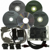
DEMO BOARD FOR 9S12NE64
Manufacturer
Freescale Semiconductor
Type
MCUr
Datasheet
1.DEMO9S12NE64E.pdf
(21 pages)
Specifications of DEMO9S12NE64E
Contents
*
Processor To Be Evaluated
MC9S12NE64
Maximum Operating Temperature
+ 50 C
Minimum Operating Temperature
- 10 C
Operating Supply Voltage
6 V to 12 V
Silicon Manufacturer
Freescale
Core Architecture
S12
Core Sub-architecture
S12
Silicon Core Number
MC9S12
Silicon Family Name
S12NE
Rohs Compliant
Yes
For Use With/related Products
MC9S12NE64
Lead Free Status / RoHS Status
Lead free / RoHS Compliant


Support Information
16
Pin
1
2
3
4
5
6
7
8
9
RESET_B
IRQ_B
PH<4>
P3_3V
PS<1>
PS<0>
PJ<0>
PJ<1>
Label
GND
Table 2-2 I/O Connector (J50) Signal Descriptions
DEMO9S12NE64 User’s Manual, Rev. 0.8
3.3 VDC supplied from the DEMO9S12NE64
IRQ_B, which is also PE1, is always an input and can always be read. This
input is used for requesting an asynchronous interrupt to the MCU. When used
as an interrupt pin, this signal is active-low
GROUND
Active low bidirectional control signal that acts as an input to initialize the
MCU to a known start-up state. It also acts as an open-drain output to indicate
that an internal failure has been detected in either the clock monitor or COP
watchdog circuit
PS1 is a general purpose input or output. When the Serial Communications
Interface 0 (SCI0) transmitter is enabled the PS1 pin is configured as the
transmit pin, TXD, of SCI0
PJ0 is a general purpose I/O pin. When the EMAC MII interface is enabled it
becomes the management data clock(MII_MDC) signal
PS0 is a general purpose input or output. When the Serial Communications
Interface 0 (SCI0) receiver is enabled the PS0 pin is configured as the receive
pin RXD0 of SCI0
PJ1 is a general purpose I/O pin. When the EMAC MII interface is enabled it
becomes the Management Data I/O (MII_MDIO) signal
PH4 is a general purpose input or output pin. When the EMAC MII interface is
enabled it becomes the transmit Clock (MII_TXCLK) signal
Figure 2-1 I/O Connector (J50) Pin Assignments
PH<4> 9
PH<5> 11
PG<0> 25
PG<1> 27
PG<2> 29
PG<3> 31
PG<4> 33
PG<5> 35
PG<6> 37
PG<7> 39
P3_3V 1
PS<1> 5
PS<0> 7
PT<4> 13
PT<5> 15
PS<5> 17
PS<4> 19
PS<6> 21
PS<7> 23
GND 3
• •
• •
• •
• •
• •
• •
• •
• •
• •
• •
• •
• •
• •
• •
• •
• •
• •
• •
• •
• •
J50
Signal
2
4
6
8
10
12
14
16
18
20
22
24
26
28
30
32
34
36
38
40
IRQ_B
RESET_B
PJ<0>
PJ<1>
PAD<0>
PAD<1>
PAD<2>
PAD<3>
PAD<4>
PAD<5>
PAD<6>
PAD<7>
PJ<6>
PJ<7>
PJ<2>
PJ<3>
PT<6>
PT<7>
PS<2>
PS<3>
Freescale Semiconductor
Related parts for DEMO9S12NE64E
Image
Part Number
Description
Manufacturer
Datasheet
Request
R

Part Number:
Description:
Manufacturer:
Freescale Semiconductor, Inc
Datasheet:
Part Number:
Description:
Manufacturer:
Freescale Semiconductor, Inc
Datasheet:
Part Number:
Description:
Manufacturer:
Freescale Semiconductor, Inc
Datasheet:
Part Number:
Description:
Manufacturer:
Freescale Semiconductor, Inc
Datasheet:
Part Number:
Description:
Manufacturer:
Freescale Semiconductor, Inc
Datasheet:
Part Number:
Description:
Manufacturer:
Freescale Semiconductor, Inc
Datasheet:
Part Number:
Description:
Manufacturer:
Freescale Semiconductor, Inc
Datasheet:
Part Number:
Description:
Manufacturer:
Freescale Semiconductor, Inc
Datasheet:
Part Number:
Description:
Manufacturer:
Freescale Semiconductor, Inc
Datasheet:
Part Number:
Description:
Manufacturer:
Freescale Semiconductor, Inc
Datasheet:
Part Number:
Description:
Manufacturer:
Freescale Semiconductor, Inc
Datasheet:
Part Number:
Description:
Manufacturer:
Freescale Semiconductor, Inc
Datasheet:
Part Number:
Description:
Manufacturer:
Freescale Semiconductor, Inc
Datasheet:
Part Number:
Description:
Manufacturer:
Freescale Semiconductor, Inc
Datasheet:
Part Number:
Description:
Manufacturer:
Freescale Semiconductor, Inc
Datasheet: