NBSG14BAEVB ON Semiconductor, NBSG14BAEVB Datasheet - Page 9
NBSG14BAEVB
Manufacturer Part Number
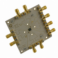
NBSG14BAEVB
Description
BOARD EVALUATION BBG NBSG14BA
Manufacturer
ON Semiconductor
Specifications of NBSG14BAEVB
Technology Type
Evaluation Board
Lead Free Status / RoHS Status
Contains lead / RoHS non-compliant
For Use With/related Products
NBSG14
Other names
NBSG14BAEVB
NBSG14BAEVBOS
NBSG14BAEVBOS


NOTE: Device will meet the specifications after thermal equilibrium has been established when mounted in a test socket or printed circuit
29. Measured using a 500 mV source, 50% duty cycle clock source. All outputs loaded with 50 W to V
30. See Figure 6. t
31. Within−Device skew is measured between outputs under identical transitions and conditions on any one device.
32. Device−to−device skew for identical transitions at identical V
33. V
34. Additive RMS Jitter with 50% duty cycle clock signal at 10 GHz.
35. Additive Peak−to−Peak data dependent jitter with NRZ PRBS 2
Table 9. AC CHARACTERISTICS for QFN−16
V
Symbol
f
t
t
t
t
V
t
t
max
PLH
PHL
SKEW
JITTER
r
f
CC
INPP
(20% − 80%)
INPP
,
= 0 V; V
board with maintained transverse airflow greater than 500 lfpm. Electrical parameters are guaranteed only over the declared
operating temperature range. Functional operation of the device exceeding these conditions is not implied. Device specification limit
values are applied individually under normal operating conditions and not valid simultaneously.
(MAX) cannot exceed V
Maximum Frequency
(See Figure 4) (Note 29)
Propagation Delay to
Output Differential
Duty Cycle Skew (Note 30)
Within−Device Skew (Note 31)
Device−to−Device Skew (Note 32)
RMS Random Clock Jitter
(Figure 4) (Note 34)
Peak−to−Peak Data Dependent Jitter
(Note 35)
Input Voltage Swing/Sensitivity
(Differential Configuration) (Note 33)
Output Rise/Fall Times
(20% − 80%) @ 1 GHz
EE
= −3.465 V to −2.375 V or V
SKEW
Characteristic
= |t
PLH
− t
CC
PHL
− V
| for a nominal 50% Differential Clock Input Waveform.
f
f
in
in
EE
< 10 Gb/s
< 10 GHz
(applicable only when V
CC
Q, Q
= 2.375 V to 3.465 V; V
10.5
Min
90
75
15
http://onsemi.com
−40°C
CC
Typ
125
0.2
12
25
30
31
3
6
levels.
CC
−1 data at 10 Gb/s.
9
−V
EE
2600
Max
EE
160
15
15
50
55
1
= 0 V
< 2600 mV).
10.5
Min
90
75
20
25°C
Typ
125
0.2
12
25
10
30
3
6
2600
Max
160
15
15
50
55
CC
1
− 2.0 V. Input edge rates 40 ps
10.5
Min
90
75
20
85°C
Typ
125
0.2
12
25
30
3
6
2600
Max
160
15
15
50
55
1
GHz
Unit
mV
ps
ps
ps
ps
Related parts for NBSG14BAEVB
Image
Part Number
Description
Manufacturer
Datasheet
Request
R

Part Number:
Description:
2.5v/3.3v Sige Differential 1 4 Clock/data Driver With Rsecl Outputs
Manufacturer:
ON Semiconductor
Datasheet:

Part Number:
Description:
Buffers & Line Drivers 2.5V/3.3V Multilevel
Manufacturer:
ON Semiconductor
Part Number:
Description:
ON Semiconductor [VOLTAGE REGULATOR]
Manufacturer:
ON Semiconductor
Datasheet:
Part Number:
Description:
357-036-542-201 CARDEDGE 36POS DL .156 BLK LOPRO
Manufacturer:
ON Semiconductor
Datasheet:
Part Number:
Description:
357-036-542-201 CARDEDGE 36POS DL .156 BLK LOPRO
Manufacturer:
ON Semiconductor
Datasheet:
Part Number:
Description:
357-036-542-201 CARDEDGE 36POS DL .156 BLK LOPRO
Manufacturer:
ON Semiconductor
Datasheet:
Part Number:
Description:
357-036-542-201 CARDEDGE 36POS DL .156 BLK LOPRO
Manufacturer:
ON Semiconductor
Datasheet:
Part Number:
Description:
357-036-542-201 CARDEDGE 36POS DL .156 BLK LOPRO
Manufacturer:
ON Semiconductor
Datasheet:
Part Number:
Description:
357-036-542-201 CARDEDGE 36POS DL .156 BLK LOPRO
Manufacturer:
ON Semiconductor
Datasheet:
Part Number:
Description:
357-036-542-201 CARDEDGE 36POS DL .156 BLK LOPRO
Manufacturer:
ON Semiconductor
Datasheet:
Part Number:
Description:
357-036-542-201 CARDEDGE 36POS DL .156 BLK LOPRO
Manufacturer:
ON Semiconductor
Datasheet:
Part Number:
Description:
357-036-542-201 CARDEDGE 36POS DL .156 BLK LOPRO
Manufacturer:
ON Semiconductor
Datasheet:
Part Number:
Description:
357-036-542-201 CARDEDGE 36POS DL .156 BLK LOPRO
Manufacturer:
ON Semiconductor
Datasheet:
Part Number:
Description:
Manufacturer:
ON Semiconductor
Datasheet: