AT89DVK-04 Atmel, AT89DVK-04 Datasheet - Page 7
AT89DVK-04
Manufacturer Part Number
AT89DVK-04
Description
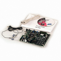
BOARD DEMO MP3 PLAYER
Manufacturer
Atmel
Datasheet
1.AT89DVK-04.pdf
(11 pages)
Specifications of AT89DVK-04
Processor To Be Evaluated
AT89C51SND1
Interface Type
USB
Lead Free Status / RoHS Status
Contains lead / RoHS non-compliant
Other names
SND1-DEMOBOARD


4206A–MP3–11/02
AT89C51SND1 Development Board
2.1.2
2.1.3
2.1.4
2.1.5
2.1.6
2.1.7
2.1.8
2.1.9
2-3
AT89C51SND1 Area
Keypad Area
Display Area
DAC Area
In-System
Programming (ISP)
Area
DataFlash Area
MultiMedia Card
(MMC) Area
USB Area
t
Table 1. J2 Pinout
The AT89C51SND1 area consists of the AT89C51SND1 product along with the follow-
ing items:
n Reset Circuit
n 16 MHz Oscillator
n PLL Filter
n Analog Reference Circuit
The keypad area consists of a 4 by 3 matrix with one key replaced by a “Keypad Lock”
switch.
The display area consists of a 2-line by 16 characters LCD display. The contrast is
adjustable using RV1 variable resistor.
The DAC area consists of a standard audio DAC embedding the headphone amplifier.
The headphone connector is standard and allows connection of all headphone types.
The ISP area contains a switch that allows the user to select the AT89C51SND1 hard-
ware condition and thus execute the embedded bootloader or to run the client
application. Note that on V2.1 board, the switch is located on the right side of the board
near J6 connector. Figure 2-3 shows the switch position to enter ISP mode.
Figure 2-3. ISP Switch Position
The DataFlash area consists of the on-board Flash memory. It is composed of four
AT45DB642 giving 32-Mb for the V2.2 board or four AT45DB321 giving 16-Mb for the
V2.1 board.
The MultiMedia Card area consists of a 2-slot connector that allows the plug-in of two
MMC cards simultaneously.
The USB area consists of a standard USB type B receptacle for the V2.2 board while
V2.1 is equipped with a mini but non-standard connector. USB is used for two different
tasks:
n Firmware upgrade for In-System Programming.
Pin Number
1
2
User’s Code Execution
User’s Code Execution
Pin Assignment
PS (+5V supply voltage)
GND (0V supply reference)
a. V2.1 Board Implementation
b. V2.2 Board Implementation
AT89C51SND1C Development Board User Guide
ISP Execution
ISP Execution
Related parts for AT89DVK-04
Image
Part Number
Description
Manufacturer
Datasheet
Request
R

Part Number:
Description:
BOARD DEV FOR AT83C24 SMART CARD
Manufacturer:
Atmel
Datasheet:

Part Number:
Description:
8-Bit Microcontroller with 4K Bytes Flash
Manufacturer:
ATMEL Corporation
Datasheet:

Part Number:
Description:
DEV KIT FOR AVR/AVR32
Manufacturer:
Atmel
Datasheet:
Part Number:
Description:
INTERVAL AND WIPE/WASH WIPER CONTROL IC WITH DELAY
Manufacturer:
ATMEL Corporation
Datasheet:
Part Number:
Description:
Low-Voltage Voice-Switched IC for Hands-Free Operation
Manufacturer:
ATMEL Corporation
Datasheet:
Part Number:
Description:
MONOLITHIC INTEGRATED FEATUREPHONE CIRCUIT
Manufacturer:
ATMEL Corporation
Datasheet:
Part Number:
Description:
AM-FM Receiver IC U4255BM-M
Manufacturer:
ATMEL Corporation
Datasheet:
Part Number:
Description:
Monolithic Integrated Feature Phone Circuit
Manufacturer:
ATMEL Corporation
Datasheet:
Part Number:
Description:
Multistandard Video-IF and Quasi Parallel Sound Processing
Manufacturer:
ATMEL Corporation
Datasheet:
Part Number:
Description:
High-performance EE PLD
Manufacturer:
ATMEL Corporation
Datasheet:
Part Number:
Description:
8-bit Flash Microcontroller
Manufacturer:
ATMEL Corporation
Datasheet:
Part Number:
Description:
2-Wire Serial EEPROM
Manufacturer:
ATMEL Corporation
Datasheet: