EVAL-AD9831EB Analog Devices Inc, EVAL-AD9831EB Datasheet - Page 10
EVAL-AD9831EB
Manufacturer Part Number
EVAL-AD9831EB
Description
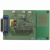
BOARD EVAL FOR AD9831
Manufacturer
Analog Devices Inc
Type
Direct Digital Synthesis (DDS)r
Datasheet
1.EVAL-AD9831EB.pdf
(16 pages)
Specifications of EVAL-AD9831EB
Contents
Evaluation Board
For Use With/related Products
AD9831
Lead Free Status / RoHS Status
Contains lead / RoHS non-compliant


AD9831
CIRCUIT DESCRIPTION
The AD9831 provides an exciting new level of integration for
the RF/Communications system designer. The AD9831 com-
bines the Numerical Controlled Oscillator (NCO), SINE Look-
Up Table, Frequency and Phase Modulators, and a Digital-to-
Analog Converter on a single integrated circuit.
The internal circuitry of the AD9831 consists of three main
sections. These are:
The AD9831 is a fully integrated Direct Digital Synthesis
(DDS) chip. The chip requires one reference clock, one low
precision resistor and eight decoupling capacitors to provide
digitally created sine waves up to 12.5 MHz. In addition to the
generation of this RF signal, the chip is fully capable of a broad
range of simple and complex modulation schemes. These
modulation schemes are fully implemented in the digital domain
allowing accurate and simple realization of complex modulation
algorithms using DSP techniques.
THEORY OF OPERATION
Sine waves are typically thought of in terms of their magnitude
form a(t) = sin ( t). However, these are nonlinear and not easy
to generate except through piece wise construction. On the
other hand, the angular information is linear in nature. That is,
the phase angle rotates through a fixed angle for each unit of
time. The angular rate depends on the frequency of the signal
by the traditional rate of
Knowing that the phase of a sine wave is linear and given a
reference interval (clock period), the phase rotation for that
period can be determined.
Solving for
Solving for f and substituting the reference clock frequency for
the reference period (1/f
The AD9831 builds the output based on this simple equation.
A simple DDS chip can implement this equation with three
major subcircuits.
Numerical Controlled Oscillator (NCO) + Phase Modulator
SINE Look-Up Table
Digital-to-Analog Converter
2
+1
–1
0
0
Figure 21. Sine Wave
f = Phase
MCLK
= Phase/ t = 2 f
= 2 f.
Phase =
= t)
MAGNITUDE
PHASE
f
MCLK
t
/2
–10–
Numerical Controlled Oscillator + Phase Modulator
This consists of two frequency select registers, a phase accumu-
lator and four phase offset registers. The main component of the
NCO is a 32-bit phase accumulator which assembles the phase
component of the output signal. Continuous time signals have a
phase range of 0 to 2 . Outside this range of numbers, the
sinusoid functions repeat themselves in a periodic manner. The
digital implementation is no different. The accumulator simply
scales the range of phase numbers into a multibit digital word.
The phase accumulator in the AD9831 is implemented with 32
bits. Therefore, in the AD9831, 2 = 2
term is scaled into this range of numbers 0 < Phase < 2
Making these substitutions into the equation above
where 0 < Phase < 2
With a clock signal of 25 MHz and a phase word of 051EB852
hex
The input to the phase accumulator (i.e., the phase step) can be
selected either from the FREQ0 Register or FREQ1 Register
and this is controlled by the FSELECT pin. NCOs inherently
generate continuous phase signals, thus avoiding any output
discontinuity when switching between frequencies.
Following the NCO, a phase offset can be added to perform
phase modulation using the 12-bit PHASE Registers. The con-
tents of this register are added to the most significant bits of the
NCO. The AD9831 has four PHASE registers, the resolution
of these registers being 2 /4096.
Sine Look-Up Table (LUT)
To make the output useful, the signal must be converted from
phase information into a sinusoidal value. Since phase informa-
tion maps directly into amplitude, a ROM LUT converts the
phase information into amplitude. To do this, the digital phase
information is used to address a sine ROM LUT. Although the
NCO contains a 32-bit phase accumulator, the output of the
NCO is truncated to 12 bits. Using the full resolution of the
phase accumulator is impractical and unnecessary as this would
require a look-up table of 2
It is necessary only to have sufficient phase resolution in the
LUTs such that the dc error of the output waveform is domi-
nated by the quantization error in the DAC. This requires the
look-up table to have two more bits of phase resolution than the
10-bit DAC.
Digital-to-Analog Converter
The AD9831 includes a high impedance current source 10-bit
DAC, capable of driving a wide range of loads at different
speeds. Full-scale output current can be adjusted, for optimum
power and external load requirements, through the use of a
single external resistor (R
The DAC is configured for single ended operation. The load
resistor can be any value required, as long as the full-scale volt-
age developed across it does not exceed the voltage compliance
range. Since full-scale current is controlled by R
ments to R
However, if the DAC full-scale output current is significantly
less than 4 mA, the DAC’s linearity may degrade.
f = 51EB852
SET
can balance changes made to the load resistor.
25 MHz/2
f = Phase
32
SET
32
).
entries.
32
= 0.500000000465 MHz
f
MCLK
32
/2
. Likewise, the Phase
32
SET
, adjust-
REV. A
32
– 1.
Related parts for EVAL-AD9831EB
Image
Part Number
Description
Manufacturer
Datasheet
Request
R

Part Number:
Description:
ENERCHIP CC EVAL KIT
Manufacturer:
Cymbet Corporation
Datasheet:

Part Number:
Description:
BOARD EVAL FOR AD976
Manufacturer:
Analog Devices Inc
Datasheet:

Part Number:
Description:
BOARD EVAL FOR ADXL345
Manufacturer:
Analog Devices Inc
Datasheet:

Part Number:
Description:
ENERCHIP CC SEH EVAL KIT
Manufacturer:
Cymbet Corporation
Datasheet:

Part Number:
Description:
ENERCHIP EP ENERGY HARVEST EVAL
Manufacturer:
Cymbet Corporation
Datasheet:

Part Number:
Description:
EVAL BOARD FOR TW6864-LB2-GR
Manufacturer:
Intersil
Datasheet:
Part Number:
Description:
EVAL BOARD FOR TW8816-LB3-GR
Manufacturer:
Intersil
Datasheet:
Part Number:
Description:
EVAL BOARD FOR TW8817-TA3-GRS
Manufacturer:
Intersil
Datasheet:

Part Number:
Description:
EVALUATION MODULE FOR ADUM4160
Manufacturer:
Analog Devices Inc
Datasheet:

Part Number:
Description:
BOARD EVALUATION ADCMP581BCP
Manufacturer:
Analog Devices Inc
Datasheet:
Part Number:
Description:
BOARD EVALUATION ADM1041
Manufacturer:
Analog Devices Inc
Datasheet:

Part Number:
Description:
EVAL BOARD FOR STM32F107VCT
Manufacturer:
STMicroelectronics
Datasheet:
Part Number:
Description:
BOARD EVAL FOR AD1954
Manufacturer:
Analog Devices Inc
Datasheet:
Part Number:
Description:
BOARD EVAL FOR AD1955
Manufacturer:
Analog Devices Inc
Datasheet:

Part Number:
Description:
BOARD EVAL FOR AD7655
Manufacturer:
Analog Devices Inc
Datasheet: