DAK-34 Power Integrations, DAK-34 Datasheet - Page 7
DAK-34
Manufacturer Part Number
DAK-34
Description
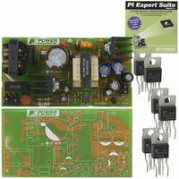
KIT DESIGN ACCELERATOR AC/DC PS
Manufacturer
Power Integrations
Series
TOPSwitch®-GXr
Specifications of DAK-34
Main Purpose
AC/DC, Primary Side
Outputs And Type
1, Isolated
Power - Output
30W
Voltage - Output
12V
Current - Output
2.5A
Voltage - Input
85 ~ 265VAC
Regulator Topology
Flyback
Frequency - Switching
132kHz
Board Type
Bare (Unpopulated) and Fully Populated
Utilized Ic / Part
TOP245
Lead Free Status / RoHS Status
Not applicable / Not applicable
Other names
596-1004


4
The schematic in Figure 2 shows an off-line flyback converter using the TOP245Y. The
circuit is designed for 85 VAC to 265 VAC input and provides an isolated 12 V, 2.5 A
output.
4.1
Capacitor CX1 and the leakage inductance of L1 filter differential mode conducted EMI.
Inductor L1 and CY1 filter common mode conducted EMI.
4.2
Rectifier bridge BR1 and C1 provide a high voltage DC supply rail for the primary
circuitry. The DC rail is applied to the primary winding of T1. The other side of the
transformer primary is driven by the integrated MOSFET in U1. Diode D1 and VR1 clamp
leakage spikes generated when the MOSFET in U1 switches off. Capacitor C2 reduces
the operating temperature of VR1 by bypassing the leading edge of the primary leakage
spike away from VR1. Resistor R3 provides damping to reduce drain ringing improving
EMI. Resistor R1 sets the low-line turn-on threshold to approximately 69 VAC and sets
the overvoltage shutdown level to approximately 320 VAC. Resistor R4 sets the U1
current limit to approximately 70% of its nominal value. Resistor R2 reduces the U1
current limit as a function of line voltage so that maximum overload power is relatively
constant (<50 W) over the entire input voltage range. This limits the output power
delivered during fault conditions. Capacitor C4 bypasses the U1 CONTROL pin while C3
has three functions. It provides the energy required by U1 during startup, sets the auto-
restart frequency during fault conditions, and also acts to roll off the gain of U1 as a
function of frequency. Resistor R5 adds a zero to the control loop to stabilize the power
supply. Diode D2 and capacitor C5 provide rectified and filtered bias power for U2 and
U1.
4.3
The secondary of T1 is rectified and filtered by D3, C6, and C7. Inductor L2 and C8
provide additional high frequency filtering. Resistor R11 and C11 provide snubbing for
D3. Choosing the proper snubber values is important for low zero-load power
consumption and for high frequency EMI suppression. The snubber components were
chosen so that the turn-on voltage spike at the D3 anode is slightly under-damped.
Increasing C11 and reducing R11 will improve damping and high frequency EMI, at the
cost of higher zero load power consumption.
4.4
Resistors R9 and R10 divide down the supply output voltage and apply it to the reference
pin of error amplifier U3. Shunt regulator U3 drives the LED of optocoupler U2 through
resistor R6 to provide feedback information to the U1 CONTROL pin. The optocoupler
output also provides power to U1 from the bias winding during normal operating
conditions. Diode D4 and capacitor C10 apply drive to the optocoupler during supply
Page 7 of 28
Circuit Description
Input EMI Filtering
TOPSwitch Primary
Output Rectification
Output Feedback
Tel: +1 408 414 9200 Fax: +1 408 414 9201
Power Integrations
www.powerint.com
Related parts for DAK-34
Image
Part Number
Description
Manufacturer
Datasheet
Request
R

Part Number:
Description:
KIT DESIGN ACCELERATOR MODEM
Manufacturer:
Power Integrations
Datasheet:

Part Number:
Description:
KIT DESIGN ACCELERATOR SET TOP
Manufacturer:
Power Integrations
Datasheet:

Part Number:
Description:
KIT REF DES DPA 6.6W DC-DC CONV
Manufacturer:
Power Integrations
Datasheet:

Part Number:
Description:
KIT DESIGN ACCELERATOR POE CONV
Manufacturer:
Power Integrations
Datasheet:

Part Number:
Description:
DESIGN ACCELERATOR KIT XT SWITCH
Manufacturer:
Power Integrations
Datasheet:

Part Number:
Description:
DESIGN ACCELERATOR KIT LP SWITCH
Manufacturer:
Power Integrations
Datasheet:

Part Number:
Description:
KIT DESIGN ACC PEAKSWITCH FAMILY
Manufacturer:
Power Integrations
Datasheet:

Part Number:
Description:
KIT DESIGN ACCELERATOR ADAPTER
Manufacturer:
Power Integrations
Datasheet:

Part Number:
Description:
KIT DESIGN ACCELERATOR ADAPTER
Manufacturer:
Power Integrations
Datasheet:

Part Number:
Description:
KIT DESIGN ACCELERATOR DC-DC
Manufacturer:
Power Integrations
Datasheet:
