EVAL-ADT7470EB Analog Devices Inc, EVAL-ADT7470EB Datasheet - Page 30
EVAL-ADT7470EB
Manufacturer Part Number
EVAL-ADT7470EB
Description
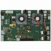
BOARD EVALUATION FOR ADT7470
Manufacturer
Analog Devices Inc
Datasheet
1.ADT7470ARQZ.pdf
(40 pages)
Specifications of EVAL-ADT7470EB
Sensor Type
Temperature
Interface
SMBus (2-Wire/I²C)
Voltage - Supply
3 V ~ 5.5 V
Embedded
No
Utilized Ic / Part
ADT7470
Lead Free Status / RoHS Status
Contains lead / RoHS non-compliant


ADT7470
Table 27. Register 0x38 to Register 0x3B. PWM Max Duty Cycle Registers (Power-On Default = 0xFF).
Register Address
0x38
0x39
0x3A
0x3B
Table 28. Register 0x3D. Device ID Register (Power-On Default = 0x70).
Register Address
0x3D
The device ID register contains the ADT7470 device ID value as a means of identifying the part over the bus.
Table 29. Register 0x3E. Company ID Register (Power-On Default = 0x41).
Register Address
0x3E
The company ID register contains 0x41, the manufacturer ID number representative of the Analog Devices, Inc. product.
Table 30. Register 0x3F. Revision Register (Power-On Default = 0x02).
Register Address
0x3F
The revision register contains the revision number of the ADT7470.
Table 31. Register 0x40. Configuration Register 1 (Power-On Default = 0x01).
Bit Name
[0] STRT
[1] Reserved
[2] Reserved
[3] TODIS
[4] LOCK
[5] FST_TCH
[6] HF_LF
[7] T05_STB
Read/Write
Read/Write
Read/Write
Read/Write
Read/Write
Read/Write
Read only
Read/Write
Read only
Read/Write
Read only
Read/Write
Read/Write
Read/Write
Read/Write
Read/Write
Read/Write
Write Once
Read/Write
Read/Write
Description
PWM1 max duty cycle: PWM1 Min duty cycle value (register 0x6A) to 100% duty cycle.
PWM2 max duty cycle: PWM2 Min duty cycle value (register 0x6B) to 100% duty cycle.
PWM3 max duty cycle: PWM3 Min duty cycle value (register 0x6C) to 100% duty cycle.
PWM4 max duty cycle: PWM4 Min duty cycle value (register 0x6D) to 100% duty cycle.
Description
Device ID.
Description
Company ID.
Description
Revision Register.
Description
Logic 1 enables monitoring and PWM control outputs based on the limit settings
programmed.
Logic 0 disables monitoring and PWM control based on the default power-up limit settings.
The limit values programmed are preserved even if a Logic 0 is written to this bit and the
default settings are enabled.
Reserved. Write 0 to this bit.
Reserved. Write 0 to this bit.
Writing a 1 disables SMBus timeout.
Once this bit is set, all lockable registers become read-only and cannot be modified until the
ADT7470 is powered down and powered up again.
Enable Fast Tach measurement.
0 = Tach measurement rate is 1 measurement per second
1= Tach measurement rate is 1 measurement every 250ms
This bit switches between high frequency and low frequency fan drive.
0 (default) = high frequency fan drive (1.4 kHz or 22.5 kHz. See Configuration Register 2,
Register 0x74, Bits [6:4]) in Table 44.
1 = low frequency fandrive (frequency determined by Configuration Register 2, Register 0x74,
Bits[6:4]) in Table 44.
Select configuration for Pin 13.
0 (default) =FULL SPEED input.
1 = TMP05 start pulse output.
Rev. C | Page 30 of 40
Related parts for EVAL-ADT7470EB
Image
Part Number
Description
Manufacturer
Datasheet
Request
R


Part Number:
Description:
BOARD EVAL FOR SI270X-A
Manufacturer:
Silicon Laboratories Inc
Datasheet:

Part Number:
Description:
BUCK CONV REF DESIGN KIT IP1201
Manufacturer:
International Rectifier
Datasheet:
Part Number:
Description:
BOARD DEMO SYNC DUAL BUCK CNVTER
Manufacturer:
International Rectifier
Datasheet:
Part Number:
Description:
BOARD DEMO SYNC BUCK CONVETER
Manufacturer:
International Rectifier
Datasheet:

Part Number:
Description:
EVALBOARD/EB Omnidirectional microphone - Analog
Manufacturer:
Analog Devices
Datasheet:
Part Number:
Description:
EVALBOARD/EB Omnidirectional microphone - Analog
Manufacturer:
Analog Devices
Datasheet:


Part Number:
Description:
BOARD EVAL LED DRIVER LT3756
Manufacturer:
Linear Technology
Datasheet:

Part Number:
Description:
BOARD EVAL FOR AD7741/7742
Manufacturer:
Analog Devices Inc
Datasheet:

Part Number:
Description:
±1.7g Dual-Axis IMEMS Accelerometer Evaluation Board
Manufacturer:
Analog Devices Inc
Datasheet:

Part Number:
Description:
IC MULTIPLIER ANALOG 8-SOIC T/R
Manufacturer:
Analog Devices Inc
Datasheet:

Part Number:
Description:
IC ANALOG MULTIPLIER 8-DIP
Manufacturer:
Analog Devices Inc
Datasheet:
Part Number:
Description:
IC ANALOG MULTIPLIER 8-SOIC
Manufacturer:
Analog Devices Inc
Datasheet:
Part Number:
Description:
IC ANALOG MULTIPLIER 8-DIP
Manufacturer:
Analog Devices Inc
Datasheet: