ADNB-7052-EV Avago Technologies US Inc., ADNB-7052-EV Datasheet - Page 18
ADNB-7052-EV
Manufacturer Part Number
ADNB-7052-EV
Description
OPTICAL MOUSE EVALUATION KIT
Manufacturer
Avago Technologies US Inc.
Series
LaserStream™r
Type
Optical Mouser
Datasheet
1.ADNB-7052-EV.pdf
(45 pages)
Specifications of ADNB-7052-EV
Contents
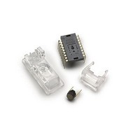
Mouse Sensor, VCSEL, Lens, Laser Assembly Clip and Documentation
Description/function
Laser Mouse Bundle
Interface Type
SPI
Product
Display Modules
Touch Panel
No Touch Panel
For Use With/related Products
ADNS-7050
Lead Free Status / Rohs Status
Details
Other names
Q2656643
Q2755626
Q2755626


SCLK
SCLK
During a read operation SCLK should be delayed at least
t
ADNS-7050 has time to prepare the requested data. The
falling edge of SCLK for the first address bit of either the
read or write command must be at least t
the last SCLK rising edge of the last data bit of the previ-
ous read operation.
Burst Mode Operation
Burst mode is a special serial port operation mode that
may be used to reduce the serial transaction time for a
motion read. The speed improvement is achieved by con-
tinuous data clocking to or from multiple registers with-
out the need to specify the register address, and by not
requiring the normal delay period between data bytes.
18
If the rising edge of the SCLK for the last data bit of the
second write command occurs before the required delay
(t
correctly.
Figure 19. Timing between write and read commands.
Figure 20. Timing between read and either write or subsequent read commands.
SCLK
Figure 21. Motion burst timing.
SRAD
SWW
MOTION_BURST REGISTER ADDRESS
), then the first write command may not complete
after the last address data bit to ensure that the
ADDRESS
ADDRESS
WRITE OPERATION
FIRST READ OPERATION
DATA
READ FIRST BYTE
t
SRAD
READ OPERATION
SRR
t
SRAD
or t
SRW
READ SECOND BYTE
after
If the rising edge of SCLK for the last address bit of the
read command occurs before the required delay (t
the write command may not complete correctly.
Burst mode is activated by reading the Motion_Burst
register. The ADNS-7050 will respond with the contents
of the Motion, Delta_X, Delta_Y, SQUAL, Shutter_Upper,
Shutter_Lower, and Maximum_Pixel registers in that or-
der. The burst transaction can be terminated anywhere
in the sequence after the Delta_X value by bringing the
NCS pin high. After sending the register address, the mi-
cro-controller must wait t
data. All data bits can be read with no delay between
bytes by driving SCLK at the normal rate. The data are
latched into the output buffer after the last address bit
is received. After the burst transmission is complete, the
micro-controller must raise the NCS line for at least t
to terminate burst mode. The serial port is not available
for use until it is reset with NCS, even for a second burst
transmission.
t
SWR
NEXT READ OPERATION
READ THIRD BYTE
DATA
ADDRESS
t
SRW
or WRITE OPERATION
• • •
& t
SRR
SRAD
NEXT READ
• • •
ADDRESS
• • •
• • •
and then begin reading
• • •
• • •
SWR
BEXIT
),
Related parts for ADNB-7052-EV
Image
Part Number
Description
Manufacturer
Datasheet
Request
R

Part Number:
Description:
Display Modules & Development Tools Bundle w/Trim Lens
Manufacturer:
Avago Technologies US Inc.

Part Number:
Description:
Display Modules & Development Tools Bundle w/Trim Lens
Manufacturer:
Avago Technologies US Inc.

Part Number:
Description:
Display Modules & Development Tools Mouse sensor
Manufacturer:
Avago Technologies US Inc.
Part Number:
Description:
Display Modules & Development Tools Mouse sensor
Manufacturer:
Avago Technologies US Inc.

Part Number:
Description:
Display Modules & Development Tools Bundle w/Trim Lens
Manufacturer:
Avago Technologies US Inc.

Part Number:
Description:
Display Modules & Development Tools Sensor+Round Lens
Manufacturer:
Avago Technologies US Inc.
Part Number:
Description:
Display Modules & Development Tools Mouse sensor
Manufacturer:
Avago Technologies US Inc.

Part Number:
Description:
Display Modules & Development Tools Mouse sensor
Manufacturer:
Avago Technologies US Inc.

Part Number:
Description:
Display Modules & Development Tools Bundle w/Trim Lens
Manufacturer:
Avago Technologies US Inc.
Part Number:
Description:
Display Modules & Development Tools Mouse sensor
Manufacturer:
Avago Technologies US Inc.

Part Number:
Description:
OPTOCOUPLER GATE DRV 2A 16-SOIC
Manufacturer:
Avago Technologies US Inc.
Datasheet:
Part Number:
Description:
OPTOCOUPLER 2CH 2.5A 16-SOIC
Manufacturer:
Avago Technologies US Inc.
Datasheet:

Part Number:
Description:
OPTOCOUPLER GATE DRV 0.4A 16SOIC
Manufacturer:
Avago Technologies US Inc.
Datasheet:

Part Number:
Description:
OPTOCOUPLER 2.0A 250KHZ 8-DIP
Manufacturer:
Avago Technologies US Inc.
Datasheet:

Part Number:
Description:
OPTOCOUPLER 2.0A 250KHZ GW 8-SMD
Manufacturer:
Avago Technologies US Inc.
Datasheet: