FEATURES
Easy to use
Simple gain setting
Solder jumper
SMA/SMB outline
Decoupled supply lines
Undedicated 10-lead SOIC pad
APPLICATIONS
Characterize the AD8220
Interface the AD8220 with other evaluation tools
Breadboard custom application circuits
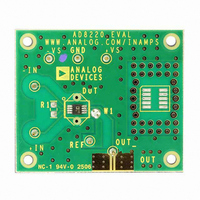
GENERAL DESCRIPTION
The AD8220-EVAL offers users the option of evaluating the
AD8220 by itself or within the context of an application. The
evaluation board is arranged such that users can easily adjust
the gain resistor and reference jumper. The board offers an
SMA/SMB outline at the output. Users can add their own
connector to interface the board with complementary tools
such as an analog-to-digital converter (ADC) evaluation board,
available from Analog Devices, Inc. Breadboard space has been
integrated to promote experimentation with the AD8220. For
example, active filters, line drivers, and converters can be placed
on the breadboard space, extending the use of the evaluation
board as a development tool.
Table 1. Factory Setting
Connection
W1 is soldered
QUICK START
Connect a ±2.3 V to ±15 V supply to +V
inputs with a signal. Measure the output on a multimeter or
oscilloscope. The output voltage is the voltage measured
between OUT and REF. The output can drive another device,
such as an ADC.
1
Rev. 0
Information furnished by Analog Devices is believed to be accurate and reliable. However, no
responsibility is assumed by Analog Devices for its use, nor for any infringements of patents or other
rights of third parties that may result from its use. Specifications subject to change without notice. No
license is granted by implication or otherwise under any patent or patent rights of Analog Devices.
Trademarks and registered trademarks are the property of their respective owners.
Assumes board is in default configuration; W1 is soldered.
1
Purpose
REF is tied to GND
S
and –V
S
. Drive the
JFET Instrumentation Amplifier
One Technology Way, P.O. Box 9106, Norwood, MA 02062-9106, U.S.A.
Tel: 781.329.4700
Fax: 781.461.3113
REFERENCE
The instrumentation amplifier’s reference level can be set by
driving the REF pin with a precision voltage reference or by
using the solder jumper, W1. By default, W1 is soldered, shunting
REF to GND. If a reference voltage other than ground is used,
the solder must be removed from W1 before driving REF with
the reference voltage, as shown in Figure 2.
+IN
–IN
5V
1V p-p, 1kHz
10µF
10µF
+IN
–IN
R1
Figure 2. Using an External Voltage Source to
Figure 1. Evaluation Board Schematic
0.1µF
+IN 4
–IN 1
R
R
0.1µF
G
G
Set the Reference Level (Circled)
3
2
10V
+
–
AD8220
©2006 Analog Devices, Inc. All rights reserved.
+
–
AD8220
DUT
+V
–V
0V
DUT
+V
S
S
8 +V
5 –V
Evaluation Board
S
W1
–V
W1
S
S
S
0.1µF
6 V
0.1µF
7 V
AD8220-EVAL
REF
REF
REF
OUT
10µF
5V
OUT
10µF
OUT
CONNECTOR
OSCILLOSCOPE
(OPTIONAL)
SMA/SMB
www.analog.com
+ COM