AD8220-EVALZ Analog Devices Inc, AD8220-EVALZ Datasheet - Page 21
AD8220-EVALZ
Manufacturer Part Number
AD8220-EVALZ
Description
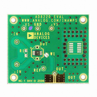
BOARD EVAL FOR AD8220ARMZ
Manufacturer
Analog Devices Inc
Specifications of AD8220-EVALZ
Design Resources
Fully Isolated Input Module Based on AD7793, ADuM5401, and a High Performance In-Amp (CN0067)
Channels Per Ic
1 - Single
Amplifier Type
Instrumentation
Output Type
Single-Ended, Rail-to-Rail
Slew Rate
2 V/µs
-3db Bandwidth
1.5MHz
Current - Output / Channel
15mA
Operating Temperature
-40°C ~ 85°C
Current - Supply (main Ic)
750µA
Voltage - Supply, Single/dual (±)
4.5 V ~ 36 V, ±2.25 V ~ 18 V
Board Type
Fully Populated
Utilized Ic / Part
AD8220
Silicon Manufacturer
Analog Devices
Application Sub Type
JFET Input Instrumentation Amplifier
Kit Application Type
Amplifier
Silicon Core Number
AD8220
Kit Contents
Board
Lead Free Status / RoHS Status
Lead free / RoHS Compliant
Other names
AD8220-EVAL
AD8220-EVAL
AD8220-EVAL


REFERENCE TERMINAL
The reference terminal, REF, is at one end of a 20 kΩ resistor
(see Figure 55). The output of the instrumentation amplifier is
referenced to the voltage on the REF terminal; this is useful
when the output signal needs to be offset to voltages other than
common. For example, a voltage source can be tied to the REF
pin to level-shift the output so that the AD8220 can interface
with an ADC. The allowable reference voltage range is a function of
the gain, common-mode input, and supply voltages. The REF
pin should not exceed either +V
For best performance, especially in cases where the output is
not measured with respect to the REF terminal, source impedance
to the REF terminal should be kept low, because parasitic
resistance can adversely affect CMRR and gain accuracy.
POWER SUPPLY REGULATION AND BYPASSING
The AD8220 has high PSRR. However, for optimal
performance, a stable dc voltage should be used to power
the instrumentation amplifier. Noise on the supply pins can
adversely affect performance. As in all linear circuits, bypass
capacitors must be used to decouple the amplifier.
A 0.1 μF capacitor should be placed close to each supply pin.
A 10 μF tantalum capacitor can be used further away from the
part (see Figure 59). In most cases, it can be shared by other
precision integrated circuits.
Figure 59. Supply Decoupling, REF and Output Referred to Ground
+IN
–IN
AD8220
+V
–V
S
S
0.1µF
0.1µF
S
or −V
REF
S
by more than 0.5 V.
10µF
10µF
LOAD
V
OUT
Rev. B | Page 21 of 28
INPUT BIAS CURRENT RETURN PATH
The AD8220 input bias current is extremely small at less than
10 pA. Nonetheless, the input bias current must have a return
path to common. When the source, such as a transformer,
cannot provide a return current path, one should be created
(see Figure 60).
INPUT PROTECTION
All terminals of the AD8220 are protected against ESD.
(ESD protection is guaranteed to 4 kV, human body model.) In
addition, the input structure allows for dc overload conditions
a diode drop above the positive supply and a diode drop below
the negative supply. Voltages beyond a diode drop of the supplies
cause the ESD diodes to conduct and enable current to flow
through the diode. Therefore, an external resistor should be
used in series with each of the inputs to limit current for
voltages above +Vs. In either scenario, the AD8220 safely
handles a continuous 6 mA current at room temperature.
For applications where the AD8220 encounters extreme
overload voltages, as in cardiac defibrillators, external series
resistors and low leakage diode clamps, such as BAV199Ls,
FJH1100s, or SP720s, should be used.
f
HIGH-PASS
=
2πRC
Figure 60. Creating an I
1
C
C
TRANSFORMER
R
R
AC-COUPLED
AD8220
BIAS
AD8220
+V
+V
–V
–V
Path
S
S
S
S
REF
REF
AD8220
Related parts for AD8220-EVALZ
Image
Part Number
Description
Manufacturer
Datasheet
Request
R

Part Number:
Description:
AD8220/1/6/8/9 MSOP Pkg Eval Bd
Manufacturer:
Analog Devices Inc
Datasheet:

Part Number:
Description:
Single Supply, Rail to Rail Low Power FET-Input Op Amp
Manufacturer:
Analog Devices
Datasheet:

Part Number:
Description:
±1.7g Dual-Axis IMEMS Accelerometer Evaluation Board
Manufacturer:
Analog Devices Inc
Datasheet:
Part Number:
Description:
Inertial Sensor Evaluation System
Manufacturer:
Analog Devices Inc
Datasheet:
Part Number:
Description:
Manufacturer:
Analog Devices Inc
Datasheet:
Part Number:
Description:
Manufacturer:
Analog Devices Inc
Datasheet:
Part Number:
Description:
Manufacturer:
Analog Devices Inc
Datasheet:
Part Number:
Description:
Manufacturer:
Analog Devices Inc
Datasheet:
Part Number:
Description:
Manufacturer:
Analog Devices Inc
Datasheet:
Part Number:
Description:
Manufacturer:
Analog Devices Inc
Datasheet:
Part Number:
Description:
Manufacturer:
Analog Devices Inc
Datasheet:
Part Number:
Description:
Manufacturer:
Analog Devices Inc
Datasheet:
Part Number:
Description:
Manufacturer:
Analog Devices Inc
Datasheet: