EVAL6599-200W STMicroelectronics, EVAL6599-200W Datasheet - Page 4
EVAL6599-200W
Manufacturer Part Number
EVAL6599-200W
Description
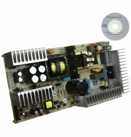
EVAL BOARD FOR L6599
Manufacturer
STMicroelectronics
Type
Power Factor Correctionr
Specifications of EVAL6599-200W
Main Purpose
AC/DC, Primary Side and PFC
Outputs And Type
4, Isolated
Power - Output
200W
Voltage - Output
24V, 12V, 5V, 3.3V
Current - Output
6A, 5A, 1A, 700mA
Voltage - Input
90 ~ 264VAC
Regulator Topology
Resonant
Frequency - Switching
95kHz
Board Type
Fully Populated
Utilized Ic / Part
L6563, L6599
Input Voltage
90 V to 264 V
Output Voltage
3.3 V to 24 V
Dimensions
132 mm x 265 mm
Product
Power Management Modules
Lead Free Status / RoHS Status
Lead free / RoHS Compliant
For Use With/related Products
L6599
Other names
497-5496


Main characteristics and circuit description
1
Note:
4/35
Main characteristics and circuit description
The main characteristics of the SMPS are listed below:
●
●
●
●
●
●
●
●
The circuit consists of three stages. A front-end PFC pre-regulator implemented by the
controller L6563
controller L6599
(Figure
The PFC stage delivers a stable 400 V
harmonics, in order to meet the requirements of the European norm EN61000-3-2 and the
JEIDA-MITI norm for Japan.
The PFC controller is the L6563 (U1), working in FOT (fixed off-time) mode and integrating
all functions needed to operate the PFC and interface the downstream resonant converter.
The FOT control is implemented through components C15, C17, D5, Q3, R14, R17 and R29
(see AN1792 for a complete description of a FOT PFC pre-regulator).
The power stage of the PFC is a conventional boost converter, connected to the output of
the rectifier bridge through a differential mode filtering cell (C5, C6 and L3) for EMI
reduction. It includes a coil (L4), diode (D3) and two capacitors (C7 and C8).
The boost switch is represented by the Power MOSFET (Q2) which is directly driven by the
L6563 output drive thanks to the high current capability of the IC.
The divider (R30, R31 and R32) provides the L6563 (MULT Pin 3) with the information of the
instantaneous voltage that is used to modulate the boost current and to derive some further
information like the average value of the AC line used by the V
function. This function is used to keep the output voltage almost independent of the mains
one.
The first divider (R3, R6, R8, R10 and R11) is dedicated to detecting the output voltage
while the second divider (R5, R7, R9, R16 and R25) is used to protect the circuit in case of
voltage loop fail.
The second stage is an LLC resonant converter, with half bridge topology, working in ZVS
(zero voltage switching) mode.
The controller is the L6599 integrated circuit that incorporates the necessary functions to
drive properly the two half-bridge MOSFETs by a 50 percent fixed duty cycle with dead-time,
Universal input mains range: 90 to 264 V
Output voltages:
–
–
–
–
Mains harmonics: Compliance with EN61000-3-2 specifications
St-by mains consumption: Typical 0.5 W @230 V
Overall efficiency: better than 88% at full load
EMI: Compliance with EN55022-class B specifications
Safety: Compliance with EN60950 specifications
PCB single layer: 132x265 mm, mixed PTH/SMT technologies
4) utilizing the VIPer12A-E off-line primary switcher.
24 V@6 A continuous operation
12 V@ 5 A continuous operation
3.3 V@ 0.7 A continuous operation
5 V@ 1 A continuous operation
(Figure
(Figure
2), a half-bridge resonant DC/DC converter based on the resonant
3) and a 7 W flyback converter intended for stand-by management
DC
supply and provides for the reduction of the mains
ac
and frequencies between 45 and 65 Hz
ac
FF
(voltage feed-forward)
AN2393
Related parts for EVAL6599-200W
Image
Part Number
Description
Manufacturer
Datasheet
Request
R

Part Number:
Description:
EVAL BOARD FOR L6599
Manufacturer:
STMicroelectronics
Datasheet:

Part Number:
Description:
DEMO BOARD FOR L6599
Manufacturer:
STMicroelectronics
Datasheet:

Part Number:
Description:
DEMO BOARD FOR L6599
Manufacturer:
STMicroelectronics
Datasheet:

Part Number:
Description:
STMicroelectronics [RIPPLE-CARRY BINARY COUNTER/DIVIDERS]
Manufacturer:
STMicroelectronics
Datasheet:
Part Number:
Description:
STMicroelectronics [LIQUID-CRYSTAL DISPLAY DRIVERS]
Manufacturer:
STMicroelectronics
Datasheet:

Part Number:
Description:
BOARD EVAL FOR MEMS SENSORS
Manufacturer:
STMicroelectronics
Datasheet:
Part Number:
Description:
NPN TRANSISTOR POWER MODULE
Manufacturer:
STMicroelectronics
Datasheet:
Part Number:
Description:
TURBOSWITCH ULTRA-FAST HIGH VOLTAGE DIODE
Manufacturer:
STMicroelectronics
Datasheet:
Part Number:
Description:
Manufacturer:
STMicroelectronics
Datasheet:
Part Number:
Description:
DIODE / SCR MODULE
Manufacturer:
STMicroelectronics
Datasheet:
Part Number:
Description:
DIODE / SCR MODULE
Manufacturer:
STMicroelectronics
Datasheet:
Part Number:
Description:
Search -----> STE16N100
Manufacturer:
STMicroelectronics
Datasheet: