EVAL6599-90W STMicroelectronics, EVAL6599-90W Datasheet - Page 5
EVAL6599-90W
Manufacturer Part Number
EVAL6599-90W
Description
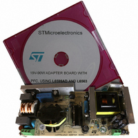
EVAL BOARD FOR L6599
Manufacturer
STMicroelectronics
Type
Power Factor Correctionr
Specifications of EVAL6599-90W
Main Purpose
AC/DC, Primary Side and PFC
Outputs And Type
1, Isolated
Power - Output
90W
Voltage - Output
19V
Current - Output
4.7A
Voltage - Input
90 ~ 264VAC
Regulator Topology
Resonant
Frequency - Switching
90kHz
Board Type
Fully Populated
Utilized Ic / Part
L6563, L6599
Input Voltage
90 V to 264 V
Output Voltage
19 V
Dimensions
78 mm x 174 mm
Product
Power Management Modules
Lead Free Status / RoHS Status
Lead free / RoHS Compliant
For Use With/related Products
L6599
Other names
497-5497
Available stocks
Company
Part Number
Manufacturer
Quantity
Price


AN2321
1
Main characteristics and circuit description
The main characteristics of the SMPS are listed here below:
●
●
●
●
●
●
●
●
●
The circuit consists of two stages: a front-end PFC implementing the L6563 and a resonant
DC/DC converter based on the new resonant controller, the L6599. The Power Factor
Corrected (PFC) stage delivers a stable 400 VDC and provides for the reduction of the
mains harmonic, allowing to meet European standard EN61000-3-2. The controller is the
L6563 (U1), working in transition mode and integrating all functions needed to control the
PFC and interface the downstream resonant converter. The power stage of the PFC is a
conventional boost converter, connected to the output of the rectifier bridge. It includes coil
L2, diode D4 and capacitor C9. The boost switch is represented by the power MOSFET Q1.
The L2 secondary winding (pins 8-10) is dedicated to provide to the L6563 the information
about the PFC coil core demagnetization, necessary to the controller for the TM operation.
The divider R1, R2 and R14 provides to the L6563 the information of the instantaneous
voltage that is used to modulate the boost current, and to derive some further information
like the average value of the AC line, used by the V
function keeps the output voltage almost independent of the mains one. The divider R7, R8,
R9, R10 detects the output voltage. The second divider R11, R12, R13 and R28 protects the
circuit in case of voltage loop fail. The second stage is a resonant converter, half bridge
topology, working in ZVS. The controller is the new L6599, incorporating the necessary
functions to drive properly the Half-bridge by a 50 percent fixed duty cycle with dead-time,
working with variable frequency.
The main features of the L6599 are a non-linear soft-start, a new current protection pin
(ISEN, pin 6) that programs the hiccup mode timing, a dedicated pin for sequencing or
brown-out (LINE) and a stand-by pin (STBY) for burst mode operation at light load. The
transformer uses the integrated magnetic approach, incorporating the resonant series
inductance. Thus, no any external additional coil is needed for the resonance. The
transformer configuration chosen for the secondary winding is centre tap, using two
Schottky rectifiers, type STPS10L60FP. The feedback loop is implemented by means of a
typical circuit using a TL431 modifying the current in the optocoupler diode. The optocoupler
transistor modulates the current from pin 4, so the frequency will change accordingly, thus
achieving the output voltage regulation. Resistor R34 sets the maximum operating
frequency and the load at which the controller starts to work in Burst mode. In case of a
short circuit, the current into the primary winding is detected by the lossless circuit R41,
C27, D11, D10, R39, and C25 and it is fed into the pin 6. In case of overload, the voltage on
pin #6 will overpass an internal threshold that will trigger a protection sequence via pin #2,
keeping the current flowing in the circuit at a safe level. In case of output voltage loop failure,
the intervention of the zener diode connected to pin #8 (DIS) will activate the latched
protection of the L6599. The DIS pin can be also activated by the L6563 via the
PWM_LATCH pin in case of PFC loop failure.
Universal input mains range: 90÷264 Vac - frequency 45 to 65 Hz
Output voltage: 19 V@4.7 A continuous operation
Mains harmonics: Compliance with EN61000-3-2 specifications
Standby mains consumption: Typ. 0.4 W @230 Vac; Max 0.5 W @265 Vac
Overall efficiency: better than 90%
EMI: Compliance with EN55022-class B specifications
Safety: Compliance with EN60950 specifications
Low profile design: 25 mm maximum height
PCB single layer: 78x174 mm, mixed PTH/SMT technologies
Main characteristics and circuit description
FF
(voltage feed-forward) function. This
5/29
Related parts for EVAL6599-90W
Image
Part Number
Description
Manufacturer
Datasheet
Request
R

Part Number:
Description:
EVAL BOARD FOR L6599
Manufacturer:
STMicroelectronics
Datasheet:

Part Number:
Description:
DEMO BOARD FOR L6599
Manufacturer:
STMicroelectronics
Datasheet:

Part Number:
Description:
DEMO BOARD FOR L6599
Manufacturer:
STMicroelectronics
Datasheet:

Part Number:
Description:
STMicroelectronics [RIPPLE-CARRY BINARY COUNTER/DIVIDERS]
Manufacturer:
STMicroelectronics
Datasheet:
Part Number:
Description:
STMicroelectronics [LIQUID-CRYSTAL DISPLAY DRIVERS]
Manufacturer:
STMicroelectronics
Datasheet:

Part Number:
Description:
BOARD EVAL FOR MEMS SENSORS
Manufacturer:
STMicroelectronics
Datasheet:
Part Number:
Description:
NPN TRANSISTOR POWER MODULE
Manufacturer:
STMicroelectronics
Datasheet:
Part Number:
Description:
TURBOSWITCH ULTRA-FAST HIGH VOLTAGE DIODE
Manufacturer:
STMicroelectronics
Datasheet:
Part Number:
Description:
Manufacturer:
STMicroelectronics
Datasheet:
Part Number:
Description:
DIODE / SCR MODULE
Manufacturer:
STMicroelectronics
Datasheet:
Part Number:
Description:
DIODE / SCR MODULE
Manufacturer:
STMicroelectronics
Datasheet:
Part Number:
Description:
Search -----> STE16N100
Manufacturer:
STMicroelectronics
Datasheet: