EVAL6599-90W STMicroelectronics, EVAL6599-90W Datasheet - Page 9
EVAL6599-90W
Manufacturer Part Number
EVAL6599-90W
Description
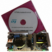
EVAL BOARD FOR L6599
Manufacturer
STMicroelectronics
Type
Power Factor Correctionr
Specifications of EVAL6599-90W
Main Purpose
AC/DC, Primary Side and PFC
Outputs And Type
1, Isolated
Power - Output
90W
Voltage - Output
19V
Current - Output
4.7A
Voltage - Input
90 ~ 264VAC
Regulator Topology
Resonant
Frequency - Switching
90kHz
Board Type
Fully Populated
Utilized Ic / Part
L6563, L6599
Input Voltage
90 V to 264 V
Output Voltage
19 V
Dimensions
78 mm x 174 mm
Product
Power Management Modules
Lead Free Status / RoHS Status
Lead free / RoHS Compliant
For Use With/related Products
L6599
Other names
497-5497
Available stocks
Company
Part Number
Manufacturer
Quantity
Price


AN2321
2.3
The transformer primary current wave shape is the CH4 trace. As shown, it is almost
sinusoidal, because the operating frequency is slightly above the resonance of the leakage
inductance and the resonant capacitor (C28).
In this condition, the circuit has a good margin for ZVS operations providing good efficiency
and the almost sinusoidal wave shape provides for an extremely low EMI generation.
Figure 4.
In
reverse voltage is measured by CH3 and the peak to peak value is indicated on the right of
the picture. It is a bit higher than the theoretical value that would be 2(V
about 40 V. It is possible to observe a small ringing on the bottom side of the waveform,
responsible for this difference. The channel CH4 (green in the picture) shows the current in
the diode D12, equal to that one flowing in D13. Even this current shape is almost a sine
wave, its average value is half of the output current. The ripple and noise on the output
voltage is measured by CH2.
Thanks to the advantages of the resonant converter, the high frequency ripple and noise of
the output voltage is only 100mV (0.52%) including spikes, while the residual ripple at mains
frequency is 130 mV at maximum load and any line condition.
Stand-by & no load power consumption
The board is specifically designed for light load and zero load operation, like during
operation with load disconnected. The results are reported in the diagram of
following. As highlighted in the diagram of
below 0.4 W for any input mains voltage. Thanks to the L6599 stand-by function, at light load
conditions both the resonant converter and the PFC work skipping switching cycles,
according to the load. In fact, the L6599 via the PFC_STOP pin (#9) stops the operation of
the L6563 during the burst mode off-time.
Figure 4
are represented some waveforms relevant to the secondary side: the rectifiers
Resonant circuit secondary side waveforms
CH2: +19V Output voltage ripple and noise
CH3: D12 rectifiers anode voltage
CH4: D12 rectifiers current
Figure
4, the input power at no load is always
OUT
+V
Figure
F
Test results
), hence
5, here
9/29
Related parts for EVAL6599-90W
Image
Part Number
Description
Manufacturer
Datasheet
Request
R

Part Number:
Description:
EVAL BOARD FOR L6599
Manufacturer:
STMicroelectronics
Datasheet:

Part Number:
Description:
DEMO BOARD FOR L6599
Manufacturer:
STMicroelectronics
Datasheet:

Part Number:
Description:
DEMO BOARD FOR L6599
Manufacturer:
STMicroelectronics
Datasheet:

Part Number:
Description:
STMicroelectronics [RIPPLE-CARRY BINARY COUNTER/DIVIDERS]
Manufacturer:
STMicroelectronics
Datasheet:
Part Number:
Description:
STMicroelectronics [LIQUID-CRYSTAL DISPLAY DRIVERS]
Manufacturer:
STMicroelectronics
Datasheet:

Part Number:
Description:
BOARD EVAL FOR MEMS SENSORS
Manufacturer:
STMicroelectronics
Datasheet:
Part Number:
Description:
NPN TRANSISTOR POWER MODULE
Manufacturer:
STMicroelectronics
Datasheet:
Part Number:
Description:
TURBOSWITCH ULTRA-FAST HIGH VOLTAGE DIODE
Manufacturer:
STMicroelectronics
Datasheet:
Part Number:
Description:
Manufacturer:
STMicroelectronics
Datasheet:
Part Number:
Description:
DIODE / SCR MODULE
Manufacturer:
STMicroelectronics
Datasheet:
Part Number:
Description:
DIODE / SCR MODULE
Manufacturer:
STMicroelectronics
Datasheet:
Part Number:
Description:
Search -----> STE16N100
Manufacturer:
STMicroelectronics
Datasheet: