HW-USB-G Xilinx Inc, HW-USB-G Datasheet - Page 10
HW-USB-G
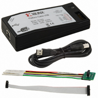
Manufacturer Part Number
HW-USB-G
Description
PLATFORM CABLE USB
Manufacturer
Xilinx Inc
Datasheet
1.HW-FLYLEADS.pdf
(20 pages)
Specifications of HW-USB-G
Accessory Type
USB Platform Cable
For Use With/related Products
Xilinx FPGA, CPLDS, Platform Flash PROMs, XC18V00 PROMs, System ACE MPM
Lead Free Status / RoHS Status
Lead free / RoHS Compliant
Other names
122-1459
HW-USB
HW-USB
HW-USB
HW-USB
Available stocks
Company
Part Number
Manufacturer
Quantity
Price


TDI_DIN_MOSI and TMS_PROG_SS Timing Specifications
For JTAG, SPI, and slave-serial configuration modes, the
TDI_DIN_MOSI and TMS_PROG_SS outputs change on
falling edges of TCK_CCLK_SCK
devices sample TDI_DIN_MOSI and TMS_PROG_SS on
rising edges of TCK_CCLK_SCK. The minimum setup time
T
TMS_PROG_SS is:
X-Ref Target - Figure 18
TDO/MISO Timing Issues
When read operations are being performed in Boundary-Scan
or SPI mode, there must be sufficient time during each one-
half clock cycle for TDO/MISO to propagate back to the cable
for sampling.
page 11
TCK_CCLK_SCK frequency is selected. An output buffer in
Platform Cable USB introduces a phase delay of 4 ns between
the cable and the target. (See cursors C1 and C2 in
page 11
The target device has a variable propagation delay from the
negative edge of TCK_CCLK_SCK to assertion of
TDO_DONE_MISO. (Refer to
TCK_CCLK_SCK to TDO_DONE_MISO delay.) For
DS300 (v3.2) May 14, 2008
Product Specification
TTSU(MIN)
T
TTSU(MIN)
illustrate a potential problem when a 24 MHz
for the CBL_TCK to TCK_CCLK_SCK delay.)
for target device sampling of TDI_DIN_MOSI or
R
Figure
Figure 18: TDI_DIN_MOSI and TMS_PROG_SS Timing with Respect to TCK_CCLK_SCK
=
=
=
19,
T
20.83 ns – 9.2 ns
11.63 ns
CLK/2
Figure 20, page
– T
Figure 20
CPD(MAX)
(Figure
TMS_PROG_SS Changes on Negative
11, and
for the
18). Target
Edge of TCK_CCLK_SCK (G1)
Figure 21,
Figure 19,
www.xilinx.com
where T
and T
TMS_PROG_SS propagation delay relative to
TCK_CCLK_SCK inherent in the output stage of the cable.
Reducing the TCK_CCLK_SCK frequency increases the
data setup time at the target.
Note:
at 24 MHz might not be possible when using a VREF below 3.3V
due to the increased propagation delay through the output buffer
stage of the cable.
example,
XC2C256-VQ100 CPLD.
Finally, signal conditioning circuitry in Platform Cable USB
introduces a third phase delay of approximately 12 ns between
TDO_DONE_MISO and the logic that samples the signal.
Note:
CBL_TDO delay.)
Data is sampled approximately 11 ns after the rising edge of
CBL_TCK. The total propagation delay must be carefully
considered to successfully operate at 24 MHz. Refer to
Figure 30, page 18
CPD(MAX)
Timing specifications apply when VREF = 3.3V. Operation
(Refer to
CLK/2
Figure 20
is the TCK_CCLK_SCK Low time at 24 MHz,
Figure 21, page 11
is the maximum TDI_DIN_MOSI or
TDI_DIN_MOSI Changes
on Negative Edge of
TCK_CCLK_SCK (G2)
for set-up timing requirements.
shows a 12 ns TDO delay for an
DS300_17_021707
for the TDO_DONE_MISO to
Platform Cable USB
10
Related parts for HW-USB-G
Image
Part Number
Description
Manufacturer
Datasheet
Request
R

Part Number:
Description:
PLATFORM CABLE USB II
Manufacturer:
Xilinx Inc
Datasheet:

Part Number:
Description:
IC CABLE
Manufacturer:
Xilinx Inc
Datasheet:

Part Number:
Description:
BOARD ADAPTER AND FLY LEADS
Manufacturer:
Xilinx Inc
Datasheet:

Part Number:
Description:
XLXHW-LICENSE-DONGLE-USB-G USB DONGLE OP
Manufacturer:
Xilinx Inc

Part Number:
Description:
KIT STARTER SPARTAN-3E
Manufacturer:
Xilinx Inc
Datasheet:
Part Number:
Description:
KIT STARTER SPARTAN-3E
Manufacturer:
Xilinx Inc
Datasheet:
Part Number:
Description:
DAUGHTER CARD VIDEO I/O VIODC
Manufacturer:
Xilinx Inc
Datasheet:
Part Number:
Description:
CoolRunner-II CPLD
Manufacturer:
XILINX [Xilinx, Inc]
Datasheet:
Part Number:
Description:
In-System Programmable CPLD
Manufacturer:
XILINX [Xilinx, Inc]
Datasheet:
Part Number:
Description:
High-Performance CPLD
Manufacturer:
XILINX [Xilinx, Inc]
Datasheet:
Part Number:
Description:
XCR3128XL 128 Macrocell CPLD
Manufacturer:
XILINX [Xilinx, Inc]
Datasheet:
Part Number:
Description:
XC95288XL High Performance CPLD
Manufacturer:
XILINX [Xilinx, Inc]
Datasheet: