TLP4006G(F) Toshiba, TLP4006G(F) Datasheet - Page 67
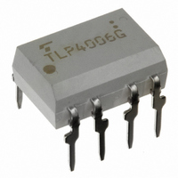
TLP4006G(F)
Manufacturer Part Number
TLP4006G(F)
Description
PHOTORELAY MOSFET OUT 3MA 8-DIP
Manufacturer
Toshiba
Series
TLP4006Gr
Specifications of TLP4006G(F)
Circuit
DPST-NO/NC (1 Form A and B)
Output Type
AC, DC
On-state Resistance
25 Ohm
Load Current
120mA
Voltage - Input
1.15VDC
Voltage - Load
0 ~ 350 V
Mounting Type
Through Hole
Termination Style
PC Pin
Package / Case
8-DIP (0.300", 7.62mm)
Input Type
DC
Input Voltage (max)
1.3V
Output Voltage (max)
350V
Input Current (max)
50mA
Output Current
120mA
Circuit Arrangement
1 Form A/1 Form B
Package Type
PDIP
Output Device
MOSFET
Pin Count
8
Mounting
Through Hole
Operating Temp Range
-40C to 85C
Operating Temperature Classification
Industrial
Rad Hardened
No
Load Voltage Rating
350 V
Load Current Rating
50 mA
Contact Form
1 Form A, 1 Form B
Mounting Style
SMD/SMT
Relay Type
Solid State
Lead Free Status / RoHS Status
Lead free / RoHS Compliant
Other names
TLP4006GF


11
1
High Speed
Low Input Current Drive
No Pull-up Resistor Required
High V
Digital Interface Applications
5 V
5 V
5 V
5 V
CC
V
Photocoupler Application Circuit Examples
V
V
V
CC
CC
CC
CC
Tolerance
15 kΩ
2 kΩ
120 pF
LSTTL
LSTTL
CMOS
1.1 kΩ
4.7 kΩ
3 mA
7.5 mA
LSTTL
390 Ω
0.5 mA
1.6 mA
TLP118, TLP2601
TLP2200
TLP558
TLP553
V
V
V
CC
CC
CC
510 kΩ
0.1 μF
0.1 μF
V
V
R
CC
CC
L
LSTTL
CMOS
0.1 μF
= 5 V
= 20 V R
1 kΩ
6.8 kΩ
R
V
V
LSTTL
LSTTL
CC
CC
L
L
5 V
= 3 kΩ
= 12 kΩ
67
V
V
CC
CC
5 V
5 V
The TLP2601 allows high-speed data
transmission at up to approximately 5 MHz.
Data rate of left-side circuit
The high-CTR (current transfer ratio) TLP553
allows operation with low input current (0.5 mA)
and direct driving with a CMOS signal.
Data rate of left-side circuit
When the TLP2200 with a 3-state output is used,
the next-stage logic gate can be actuated
without using a pull-up resistor.
Data rate of left-side circuit
By using the TLP558 which tolerates V
20 V, CMOS logic gates and other components
can be driven without design restrictions on V
Data rate of left-side circuit
f (typ.): 5 Mbit/s (duty cycle ≅ 1/2)
f (typ.): 50 kbit/s (duty cycle ≅ 1/2)
f (typ.): 1 Mbit/s (duty cycle ≅ 1/2)
f (typ.): 1 Mbit/s (duty cycle ≅ 1/2)
CC
up to
CC
.
Related parts for TLP4006G(F)
Image
Part Number
Description
Manufacturer
Datasheet
Request
R


Part Number:
Description:
Toshiba Semiconductor [TOSHIBA IGBT Module Silicon N Channel IGBT]
Manufacturer:
TOSHIBA Semiconductor CORPORATION
Datasheet:
Part Number:
Description:
TOSHIBA GTR MODULE SILICON NPN TRIPLE DIFFUSED TYPE
Manufacturer:
TOSHIBA Semiconductor CORPORATION
Datasheet:
Part Number:
Description:
TOSHIBA GTR Module Silicon N Channel IGBT
Manufacturer:
TOSHIBA Semiconductor CORPORATION
Datasheet:
Part Number:
Description:
TOSHIBA Intelligent Power Module Silicon N Channel IGBT
Manufacturer:
TOSHIBA Semiconductor CORPORATION
Datasheet:
Part Number:
Description:
TOSHIBA INTELLIGENT POWER MODULE SILICON N CHANNEL LGBT
Manufacturer:
TOSHIBA Semiconductor CORPORATION
Datasheet:
Part Number:
Description:
TOSHIBA IGBT Module Silicon N Channel IGBT
Manufacturer:
TOSHIBA Semiconductor CORPORATION
Datasheet:
Part Number:
Description:
TOSHIBA GTR MODULE SILICON N−CHANNEL IGBT
Manufacturer:
TOSHIBA Semiconductor CORPORATION
Datasheet:
Part Number:
Description:
TOSHIBA Intelligent Power Module Silicon N Channel IGBT
Manufacturer:
TOSHIBA Semiconductor CORPORATION
Datasheet:
Part Number:
Description:
TOSHIBA GTR Module Silicon N Channel IGBT
Manufacturer:
TOSHIBA Semiconductor CORPORATION
Datasheet:
Part Number:
Description:
TOSHIBA INTELLIGENT POWER MODULE
Manufacturer:
TOSHIBA Semiconductor CORPORATION
Datasheet:
Part Number:
Description:
TOSHIBA Intelligent Power Module Silicon N Channel IGBT
Manufacturer:
TOSHIBA Semiconductor CORPORATION
Datasheet:
Part Number:
Description:
TOSHIBA Intelligent Power Module Silicon N Channel IGBT
Manufacturer:
TOSHIBA Semiconductor CORPORATION
Datasheet:
Part Number:
Description:
TOSHIBA IGBT Module Silicon N Channel IGBT
Manufacturer:
TOSHIBA Semiconductor CORPORATION
Datasheet:
Part Number:
Description:
TOSHIBA Intelligent Power Module Silicon N Channel IGBT
Manufacturer:
TOSHIBA Semiconductor CORPORATION
Datasheet: