ASSR-4110-003E Avago Technologies US Inc., ASSR-4110-003E Datasheet
ASSR-4110-003E
Specifications of ASSR-4110-003E
Available stocks


Related parts for ASSR-4110-003E


ASSR-4110-003E Summary of contents
Page 1
... Single and Dual Channel Normally-off Single-Pole- Single-Throw (SPST) Relay • 400V Output Withstand Voltage • 0.12A or 0.24A Current Rating (See Schematic for ASSR-4111 Connection A and B) • Low Input Current: CMOS Compatibility • Low On-Resistance: 5.5Ω Typical for DC-only, 16Ω Typical for AC/DC • ...
Page 2
... Ordering Information ASSR-xxxx is UL Recognized with 3750 Vrms for 1 minute per UL1577 and is approved under CSA Component Ac- ceptance Notice #5, File CA 88324. Option Part number RoHS Compliant -003E ASSR-4110 -503E -001E ASSR-4111 -301E -501E -002E ASSR-4120 -302E -502E ASSR-4130 -005E (Preliminary Product ...
Page 3
... ASSR-4111 Connection A Opto -isolation Opto -isolation ASSR-4111 Connection B Opto -isolation ASSR-4120 and ASSR-4130 Opto-isolation Opto -isolation Opto -isolation 1 1 Equivalent Equivalent Relay Relay Vo Vo Diagram Diagram 2 2 Opto -isolation Equivalent 5 Relay - Diagram 2 Opto-isolation 1 2 Equivalent Relay Diagram and ...
Page 4
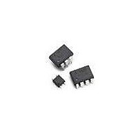
... Package Outline Drawings ASSR-4110 4-Pin Small Outline Package 2.54 (0.100) LEAD FREE xxxx 4.40±0.20 YWW (0.173±0.008) (0.268±0.016) 0.375 0.41 (0.015) (0.016) 4.3±0.2 (0.169±0.008) DIMENSIONS IN MILLIMETERS AND (INCHES) OPTION NUMBER 500 AND UL RECOGNITION NOT MARKED ASSR-4111 6-Pin DIP Package 9 ...
Page 5
... ASSR-4111 6-Pin DIP Package with Gull Wing Surface Mount Option 300 9.65 ± 0.25 (0.380 ± 0.010) 6.35 ± 0.25 (0.250 ± 0.010) 1.78 (0.070) MAX. 4.19 MAX. (0.165) 2.54 (0.100) 2.29 TYP. (0.090) NOTE: FLOATING LEAD PROTRUSION IS 0.25 mm (10 mils) MAX. ...
Page 6
... ASSR-4120 8-Pin DIP Package with Gull Wing Surface Mount Option 300 9.65 ± 0.25 (0.380 ± 0.010 1.19 (0.047) MAX. 1.080 ± 0.320 (0.043 ± 0.013) 2.54 (0.100) BSC DIMENSIONS IN MILLIMETERS (INCHES). LEAD COPLANARITY = 0.10 mm (0.004 INCHES). NOTE: FLOATING LEAD PROTRUSION IS 0.25 mm (10 mils) MAX. ...
Page 7
... C T smax smin Non-halide flux should be used. Regulatory Information The ASSR-4110, ASSR-4111, ASSR-4120 and ASSR-4130 (Preliminary Product Release) are approved by the following organizations: UL Approvals under UL 1577, component recognition program Approvals under CSA Component Acceptance Notice #5. Insulation and Safety Related Specifications ...
Page 8
... ASSR-4120 and ASSR-4130 Output Power Dissipation ASSR-4110 ASSR-4111 ASSR-4120 and ASSR-4130 Average Output Current ≤ 25°C, T 100° ASSR-4111 Con- nection B Output Voltage (T = 25°C) A ASSR-4111 Con- nection B Solder Reflow Temperature Profile Recommended Operating Conditions Parameter Symbol Input Current (ON) I F(ON) ...
Page 9
... Voltage Output Leakage I O(OFF) Current Output Offset |V | (OS) Voltage Input Reverse V R Breakdown Voltage Input Forward V F Voltage Output R (ON) On-resistance ASSR-4111 Con- nection B 9 Min. Typ. Max. Units 3750 Vrms Ω 0.4 pF 0.5 pF 0 5mA to 10mA, unless otherwise specified. F Min ...
Page 10
... ASSR-4110 - pin 1, 2 shorted and pin 3, 4 shorted. ASSR-4111 - pin shorted and pin shorted. ASSR-4120 and ASSR-4130 - pin shorted and pin shorted. 5. The Input-Output Momentary Withstand Voltage is a dielectric voltage rating that should not be interpreted as an input-output continuous voltage rating. For the continuous voltage rating refer to the IEC/EN/DIN EN 60747-5-2 Insulation Characteristics Table (if applicable), your equipment level safety specification, or Avago Technologies Application Note 1074, “ ...
Page 11
... Rss includes the effects of the temperature rise in the device 10mA, 4-Layer Board F 0.12 0.08 Safe Operating Area 0.04 0 -40 - TEMPERATURE - A Figure 1. Maximum Output Current Rating vs Ambient Temperature (ASSR-4110-003E) 0. 10mA, 4-Layer Board F 0.20 0.16 Safe 0.12 Operating Area 0.08 0.04 0 -40 - TEMPERATURE - A Figure 3 ...
Page 12
I =250µ =0.8V F 1.05 1 0.95 0.9 -50 - TEMPERATURE - A Figure 5. Normalized Typical Output Withstand Voltage vs. Temperature 1.5 1.4 I =10mA F 1.3 1.2 I =5mA F 1.1 ...
Page 13
I - INPUT CURRENT - mA F(ON) Figure 11. Typical Turn On Time vs. Input Current ...
Page 14
... PULSE GEN Ω 5ns ASSR-4120 INPUT MONITORING 2 NODE R 200ohm 3 4 INPUT 50 OUTPUT Vo 10 Figure 16. Switching Test circuit for OFF INCLUDES PROBE AND STRAY WIRING 6 5 50% P. 90% t OUTPUT Vo MONITORING NODE IS APPROXIMATELY 25pF WHICH L CAPACITANCE) OFF ...
Page 15
... ASSR-4120 1 INPUT OPEN 90% V PEAK 10 (MAX) < (0.8 OVERSHOOT ON V Figure 17. Output Transient Rejection Test Circuit PEAK 7 + PULSE GEN Ω INCLUDES PROBE AND FIXTURE CAPACITANCE M R INCLUDES PROBE AND FIXTURE RESISTANCE M 90 (0.8)V PEAK PEAK < 10% _ PEAK OUTPUT Vo MONITORING NODE 10% ...
Page 16
... For product information and a complete list of distributors, please go to our web site: Avago, Avago Technologies, and the A logo are trademarks of Avago Technologies in the United States and other countries. Data subject to change. Copyright © 2005-2008 Avago Technologies. All rights reserved. Obsoletes AV02-0279EN - September 16, 2008 V DD ASSR-4120 ...