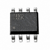
IRF7425 International Rectifier, IRF7425 Datasheet

IRF7425
Specifications of IRF7425
Available stocks
Related parts for IRF7425
IRF7425 Summary of contents
Page 1
... Thermal Resistance Parameter R Maximum Junction-to-Ambient JA www.irf.com HEXFET V R DSS DS(on) 20V 8.2@V 13 Top View Max. @ -4. -4. 150 Max. PD- 94022A IRF7425 ® Power MOSFET max ( -4.5V -15A GS = -2.5V -13A SO-8 Units -20 V -15 -12 A -60 2.5 W 1.6 20 mW/°C ± °C Units 50 °C/W ...
Page 2
... IRF7425 Electrical Characteristics @ T Parameter V Drain-to-Source Breakdown Voltage (BR)DSS Breakdown Voltage Temp. Coefficient (BR)DSS J R Static Drain-to-Source On-Resistance DS(on) V Gate Threshold Voltage GS(th) g Forward Transconductance fs I Drain-to-Source Leakage Current DSS Gate-to-Source Forward Leakage I GSS Gate-to-Source Reverse Leakage Q Total Gate Charge g Q Gate-to-Source Charge ...
Page 3
... BOTTOM 10 1 ° 0.1 0.1 100 Fig 2. Typical Output Characteristics 2 1.5 1.0 0.5 = -15V 0.0 2.0 2.2 -60 -40 -20 Fig 4. Normalized On-Resistance IRF7425 VGS -7.0V -5.0V -4.5V -2.5V -1.8V -1.5V -1.2V -1.0V -1.0V 20µs PULSE WIDTH T = 150 C ° Drain-to-Source Voltage (V) DS -15A ...
Page 4
... IRF7425 12000 1MHz iss rss gd 10000 oss iss 8000 6000 4000 C oss 2000 C rss Drain-to-Source Voltage (V) DS Fig 5. Typical Capacitance Vs. Drain-to-Source Voltage 100 10 ° 150 0.1 0.2 0.4 0.6 -V ,Source-to-Drain Voltage (V) SD Fig 7. Typical Source-Drain Diode Forward Voltage SHORTED 100 0 Fig 6 ...
Page 5
... RESPONSE) 0.01 0.00001 0.0001 Fig 11. Maximum Effective Transient Thermal Impedance, Junction-to-Ambient www.irf.com Fig 10a. Switching Time Test Circuit V GS 10% 125 150 ° 90 Fig 10b. Switching Time Waveforms 0.001 0.01 0 Rectangular Pulse Duration (sec) 1 IRF7425 D.U. Pulse Width µs Duty Factor ...
Page 6
... IRF7425 0.015 0.010 0.005 1.0 2.0 3.0 -V GS, Gate -to -Source Voltage (V) Fig 12. Typical On-Resistance Vs. Gate Voltage Charge Fig 14a. Basic Gate Charge Waveform 6 0.010 0.009 0.008 0.007 -15A 0.006 0.005 4.0 5.0 0 Fig 13. Typical On-Resistance Vs. 12V V GS Fig 14b. Gate Charge Test Circuit ...
Page 7
... Temperature ( °C ) Fig 15. Typical Vgs(th) Variance Vs. Juction Temperature www.irf.com 120 100 -250µ 100 125 150 0.001 Fig 16. Typical Power Vs. Time IRF7425 0.010 0.100 1.000 10.000 100.000 Time (sec) 7 ...
Page 8
... IRF7425 SO-8 Package Details 0.25 [.010 0.25 [.010 NOTES: 1. DIMENSIONING & TOLERANCING PER ASME Y14.5M-1994. 2. CONTROLLING DIMENSION: MILLIMETER 3. DIMENSIONS ARE SHOWN IN MILLIMETERS [INCHES]. 4. OUTLINE CONFORMS TO JEDEC OUTLINE MS-012AA. 5 DIMENSION DOES NOT INCLUDE MOLD PROTRUSIONS. MOLD PROTRUSIONS NOT TO EXCEED 0.15 [.006]. 6 DIMENSION DOES NOT INCLUDE MOLD PROTRUSIONS. ...
Page 9
... Data and specifications subject to change without notice. This product has been designed and qualified for the consumer market. Qualification Standards can be found on IR’s Web site. Visit us at www.irf.com for sales contact information. 11/01 IRF7425 12.3 ( .484 ) 11.7 ( .461 ) 14.40 ( .566 ) 12 ...


