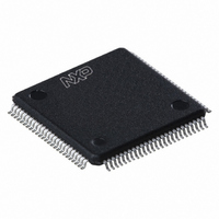
LPC2364FBD100,551 NXP Semiconductors, LPC2364FBD100,551 Datasheet - Page 30

LPC2364FBD100,551
Manufacturer Part Number
LPC2364FBD100,551
Description
IC ARM7 MCU FLASH 128K 100LQFP
Manufacturer
NXP Semiconductors
Series
LPC2300r
Datasheet
1.LPC2364FBD100551.pdf
(59 pages)
Specifications of LPC2364FBD100,551
Program Memory Type
FLASH
Program Memory Size
128KB (128K x 8)
Package / Case
100-LQFP
Core Processor
ARM7
Core Size
16/32-Bit
Speed
72MHz
Connectivity
CAN, Ethernet, I²C, Microwire, SPI, SSI, SSP, UART/USART, USB
Peripherals
Brown-out Detect/Reset, DMA, I²S, POR, PWM, WDT
Number Of I /o
70
Ram Size
34K x 8
Voltage - Supply (vcc/vdd)
3 V ~ 3.6 V
Data Converters
A/D 6x10b; D/A 1x10b
Oscillator Type
Internal
Operating Temperature
-40°C ~ 85°C
Processor Series
LPC23
Core
ARM7TDMI-S
Data Bus Width
16 bit, 32 bit
Data Ram Size
34 KB
Interface Type
CAN/I2C/I2S/SPI/SSP/UART/USB
Maximum Clock Frequency
72 MHz
Number Of Programmable I/os
70
Number Of Timers
4
Operating Supply Voltage
3.3 V
Maximum Operating Temperature
+ 85 C
Mounting Style
SMD/SMT
3rd Party Development Tools
MDK-ARM, RL-ARM, ULINK2, SAB-TFBGA100
Minimum Operating Temperature
- 40 C
On-chip Adc
6-ch x 10-bit
On-chip Dac
1-ch x 10-bit
Package
100LQFP
Device Core
ARM7TDMI-S
Family Name
LPC2000
Maximum Speed
72 MHz
Lead Free Status / RoHS Status
Lead free / RoHS Compliant
For Use With
622-1022 - BOARD SCKT ADAPTER FOR TFBGA100568-4310 - EVAL BOARD LPC2158 W/LCDMCB2360UME - BOARD EVAL MCB2360 + ULINK-MEMCB2360U - BOARD EVAL MCB2360 + ULINK2622-1019 - BOARD FOR LPC2106 48-LQFP568-4014 - BOARD EVAL FOR LPC236X ARM568-3999 - BOARD EVAL FOR LPC23 ARM MCU622-1005 - USB IN-CIRCUIT PROG ARM7 LPC2K
Eeprom Size
-
Lead Free Status / Rohs Status
Lead free / RoHS Compliant
Other names
568-3995
935282463551
LPC2364FBD100-S
935282463551
LPC2364FBD100-S
Available stocks
Company
Part Number
Manufacturer
Quantity
Price
Company:
Part Number:
LPC2364FBD100,551
Manufacturer:
NS
Quantity:
547
Company:
Part Number:
LPC2364FBD100,551
Manufacturer:
NXP Semiconductors
Quantity:
10 000
NXP Semiconductors
LPC2364_65_66_67_68_6
Product data sheet
7.24.1.1 Internal RC oscillator
7.24.1.2 Main oscillator
7.24.1.3 RTC oscillator
7.24.2 PLL
7.24.3 Wake-up timer
The IRC may be used as the clock source for the WDT, and/or as the clock that drives the
PLL and subsequently the CPU. The nominal IRC frequency is 4 MHz. The IRC is
trimmed to ±1 % accuracy.
Upon power-up or any chip reset, the LPC2364/65/66/67/68 uses the IRC as the clock
source. Software may later switch to one of the other available clock sources.
The main oscillator can be used as the clock source for the CPU, with or without using the
PLL. The main oscillator operates at frequencies of 1 MHz to 25 MHz. This frequency can
be boosted to a higher frequency, up to the maximum CPU operating frequency, by the
PLL. The clock selected as the PLL input is PLLCLKIN. The ARM processor clock
frequency is referred to as CCLK elsewhere in this document. The frequencies of
PLLCLKIN and CCLK are the same value unless the PLL is active and connected. The
clock frequency for each peripheral can be selected individually and is referred to as
PCLK. Refer to
The RTC oscillator can be used as the clock source for the RTC and/or the WDT. Also, the
RTC oscillator can be used to drive the PLL and the CPU.
The PLL accepts an input clock frequency in the range of 32 kHz to 50 MHz. The input
frequency is multiplied up to a high frequency, then divided down to provide the actual
clock used by the CPU and the USB block. The USB block is available in LPC2364/66/68
only.
The PLL input, in the range of 32 kHz to 50 MHz, may initially be divided down by a value
‘N’, which may be in the range of 1 to 256. This input division provides a wide range of
output frequencies from the same input frequency.
Following the PLL input divider is the PLL multiplier. This can multiply the input divider
output through the use of a Current Controlled Oscillator (CCO) by a value ‘M’, in the
range of 1 through 32768. The resulting frequency must be in the range of 275 MHz to
550 MHz. The multiplier works by dividing the CCO output by the value of M, then using a
phase-frequency detector to compare the divided CCO output to the multiplier input. The
error value is used to adjust the CCO frequency.
The PLL is turned off and bypassed following a chip Reset and by entering Power-down
mode. PLL is enabled by software only. The program must configure and activate the PLL,
wait for the PLL to Lock, then connect to the PLL as a clock source.
The LPC2364/65/66/67/68 begins operation at power-up and when awakened from
Power-down and Deep power-down modes by using the 4 MHz IRC oscillator as the clock
source. This allows chip operation to resume quickly. If the main oscillator or the PLL is
needed by the application, software will need to enable these features and wait for them
to stabilize before they are used as a clock source.
Section 7.24.2
Rev. 06 — 1 February 2010
for additional information.
LPC2364/65/66/67/68
Single-chip 16-bit/32-bit microcontrollers
© NXP B.V. 2010. All rights reserved.
30 of 59


