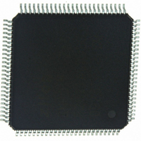
Z16F2811AL20SG Zilog, Z16F2811AL20SG Datasheet - Page 260

Z16F2811AL20SG
Manufacturer Part Number
Z16F2811AL20SG
Description
IC ZNEO MCU FLASH 128K 100LQFP
Manufacturer
Zilog
Series
Encore!® ZNEOr
Specifications of Z16F2811AL20SG
Core Processor
ZNEO
Core Size
16-Bit
Speed
20MHz
Connectivity
EBI/EMI, I²C, IrDA, LIN, SPI, UART/USART
Peripherals
Brown-out Detect/Reset, DMA, POR, PWM, WDT
Number Of I /o
76
Program Memory Size
128KB (128K x 8)
Program Memory Type
FLASH
Ram Size
4K x 8
Voltage - Supply (vcc/vdd)
2.7 V ~ 3.6 V
Data Converters
A/D 12x10b
Oscillator Type
Internal
Operating Temperature
0°C ~ 70°C
Package / Case
100-LQFP
Processor Series
Z16F2x
Core
Zneo
Data Bus Width
16 bit
Data Ram Size
4 B
Interface Type
ESPI, I2C, UART
Maximum Clock Frequency
20 MHz
Number Of Programmable I/os
76
Number Of Timers
4
Operating Supply Voltage
2.7 V to 3.6 V
Maximum Operating Temperature
+ 70 C
Mounting Style
SMD/SMT
Development Tools By Supplier
Z16F2800100ZCOG
Minimum Operating Temperature
0 C
On-chip Adc
10 bit, 12 Channel
For Use With
770-1003 - ISP 4PORT FOR ZILOG ZNEO MCU269-4537 - DEV KIT FOR Z16F ZNEO
Lead Free Status / RoHS Status
Lead free / RoHS Compliant
Eeprom Size
-
Lead Free Status / Rohs Status
Details
Other names
269-4533
Available stocks
Company
Part Number
Manufacturer
Quantity
Price
Company:
Part Number:
Z16F2811AL20SG
Manufacturer:
VISHAY
Quantity:
9 487
Part Number:
Z16F2811AL20SG
Manufacturer:
ZILOG
Quantity:
20 000
- Current page: 260 of 388
- Download datasheet (22Mb)
ADC Overview
Architecture
Operation
PS022008-0810
ADC Output = 1024*(ANAx/VREF)
The ZNEO Z16F Series devices include a 12-channel ADC. The ADC converts an analog
input signal to a 10-bit binary number. The features of the successive approximation ADC
include:
•
•
•
•
•
•
•
•
The architecture as illustrated in
plexer, sample-and-hold amplifier, and 10-bit successive approximation ADC. The ADC
digitizes the signal on selected channel and stores the digitized data in the ADC data regis-
ters. In environment with high electrical noise, an external RC filter must be added at the
input pins to reduce high frequency noise.
The ADC converts the analog input, ANAx, to a 10-bit digital representation.
The equation for calculating the digital value is represented by:
Assuming zero gain and offset errors, any voltage outside the ADC input limits of AVSS
and VREF returns all 0s or 1s, respectively.
A new conversion is initiated by either software write to the ADC Control register’s
START bit or by PWM trigger. For detailed information on the PWM trigger,
see
any conversion currently in progress and begins a new conversion. To avoid disrupting a
conversion already in progress, the START bit is read to indicate ADC operation status
(busy or available).
12 analog input sources multiplexed with GPIO ports.
Fast conversion time (2.5 s).
Programmable timing controls.
Interrupt on conversion complete.
Internal voltage reference generator.
Internal reference voltage available externally.
Ability to supply external reference voltage.
Ability to do simultaneous or independent conversions.
Synchronization of PWM and ADC
P R E L I M I N A R Y
Figure 51
on page 120. Initiating a new conversion stops
on page 243 consists of an 12-input multi-
Product Specification
ZNEO
Analog Functions
Z16F Series
244
Related parts for Z16F2811AL20SG
Image
Part Number
Description
Manufacturer
Datasheet
Request
R

Part Number:
Description:
High Performance Microcontrollers
Manufacturer:
ZiLOG Semiconductor
Datasheet:

Part Number:
Description:
Communication Controllers, ZILOG INTELLIGENT PERIPHERAL CONTROLLER (ZIP)
Manufacturer:
Zilog, Inc.
Datasheet:

Part Number:
Description:
KIT DEV FOR Z8 ENCORE 16K TO 64K
Manufacturer:
Zilog
Datasheet:

Part Number:
Description:
KIT DEV Z8 ENCORE XP 28-PIN
Manufacturer:
Zilog
Datasheet:

Part Number:
Description:
DEV KIT FOR Z8 ENCORE 8K/4K
Manufacturer:
Zilog
Datasheet:

Part Number:
Description:
KIT DEV Z8 ENCORE XP 28-PIN
Manufacturer:
Zilog
Datasheet:

Part Number:
Description:
DEV KIT FOR Z8 ENCORE 4K TO 8K
Manufacturer:
Zilog
Datasheet:

Part Number:
Description:
CMOS Z8 microcontroller. ROM 16 Kbytes, RAM 256 bytes, speed 16 MHz, 32 lines I/O, 3.0V to 5.5V
Manufacturer:
Zilog, Inc.
Datasheet:

Part Number:
Description:
Low-cost microcontroller. 512 bytes ROM, 61 bytes RAM, 8 MHz
Manufacturer:
Zilog, Inc.
Datasheet:

Part Number:
Description:
Z8 4K OTP Microcontroller
Manufacturer:
Zilog, Inc.
Datasheet:

Part Number:
Description:
CMOS SUPER8 ROMLESS MCU
Manufacturer:
Zilog, Inc.
Datasheet:

Part Number:
Description:
SL1866 CMOSZ8 OTP Microcontroller
Manufacturer:
Zilog, Inc.
Datasheet:

Part Number:
Description:
SL1866 CMOSZ8 OTP Microcontroller
Manufacturer:
Zilog, Inc.
Datasheet:

Part Number:
Description:
OTP (KB) = 1, RAM = 125, Speed = 12, I/O = 14, 8-bit Timers = 2, Comm Interfaces Other Features = Por, LV Protect, Voltage = 4.5-5.5V
Manufacturer:
Zilog, Inc.
Datasheet:


