C8051F321-GMR Silicon Laboratories Inc, C8051F321-GMR Datasheet - Page 198
C8051F321-GMR
Manufacturer Part Number
C8051F321-GMR
Description
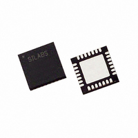
IC 8051 MCU 16K FLASH 28MLP
Manufacturer
Silicon Laboratories Inc
Series
C8051F32xr
Specifications of C8051F321-GMR
Core Processor
8051
Core Size
8-Bit
Speed
25MHz
Connectivity
SMBus (2-Wire/I²C), SPI, UART/USART, USB
Peripherals
Brown-out Detect/Reset, POR, PWM, Temp Sensor, WDT
Number Of I /o
21
Program Memory Size
16KB (16K x 8)
Program Memory Type
FLASH
Ram Size
2.25K x 8
Voltage - Supply (vcc/vdd)
2.7 V ~ 3.6 V
Data Converters
A/D 13x10b
Oscillator Type
Internal
Operating Temperature
-40°C ~ 85°C
Package / Case
28-VQFN Exposed Pad, 28-HVQFN, 28-SQFN, 28-DHVQFN
Processor Series
C8051F3x
Core
8051
Data Bus Width
8 bit
Data Ram Size
2.25 KB
Interface Type
I2C, SMBus, SPI, UART, USB
Maximum Clock Frequency
25 MHz
Number Of Programmable I/os
21
Number Of Timers
4
Maximum Operating Temperature
+ 85 C
Mounting Style
SMD/SMT
3rd Party Development Tools
PK51, CA51, A51, ULINK2
Development Tools By Supplier
C8051F320DK
Minimum Operating Temperature
- 40 C
On-chip Adc
10 bit, 13 Channel / 10 bit, 7 Channel
Package
28MLP
Device Core
8051
Family Name
C8051F321
Maximum Speed
25 MHz
Operating Supply Voltage
3.3 V
For Use With
336-1480 - DAUGHTER CARD TOOLSTCK C8051F321336-1449 - ADAPTER PROGRAM TOOLSTICK F321336-1260 - DEV KIT FOR C8051F320/F321
Lead Free Status / RoHS Status
Lead free / RoHS Compliant
Eeprom Size
-
Lead Free Status / Rohs Status
Details
Available stocks
Company
Part Number
Manufacturer
Quantity
Price

Part Number:
C8051F321-GMR
Manufacturer:
SILICON LABS/èٹ¯ç§‘
Quantity:
20 000


C8051F320/1
18.3. SPI0 Slave Mode Operation
When SPI0 is enabled and not configured as a master, it will operate as a SPI slave. As a slave, bytes are
shifted in through the MOSI pin and out through the MISO pin by a master device controlling the SCK sig-
nal. A bit counter in the SPI0 logic counts SCK edges. When 8 bits have been shifted through the shift reg-
ister, the SPIF flag is set to logic 1, and the byte is copied into the receive buffer. Data is read from the
receive buffer by reading SPI0DAT. A slave device cannot initiate transfers. Data to be transferred to the
master device is pre-loaded into the shift register by writing to SPI0DAT. Writes to SPI0DAT are double-
buffered, and are placed in the transmit buffer first. If the shift register is empty, the contents of the transmit
buffer will immediately be transferred into the shift register. When the shift register already contains data,
the SPI will load the shift register with the transmit buffer’s contents after the last SCK edge of the next (or
current) SPI transfer.
198
Figure 18.4. 4-Wire Single Master Mode and 4-Wire Slave Mode Connection
Figure 18.3. 3-Wire Single Master and Slave Mode Connection Diagram
Figure 18.2. Multiple-Master Mode Connection Diagram
Device 1
Master
Master
Device
Master
Device
GPIO
MISO
MOSI
GPIO
MISO
MOSI
MISO
MOSI
NSS
SCK
SCK
SCK
NSS
Diagram
Rev. 1.4
GPIO
MISO
MOSI
SCK
NSS
MISO
MOSI
SCK
MISO
MOSI
SCK
NSS
MISO
MOSI
SCK
NSS
Device 2
Master
Device
Device
Device
Slave
Slave
Slave
Related parts for C8051F321-GMR
Image
Part Number
Description
Manufacturer
Datasheet
Request
R

Part Number:
Description:
SMD/C°/SINGLE-ENDED OUTPUT SILICON OSCILLATOR
Manufacturer:
Silicon Laboratories Inc
Part Number:
Description:
Manufacturer:
Silicon Laboratories Inc
Datasheet:
Part Number:
Description:
N/A N/A/SI4010 AES KEYFOB DEMO WITH LCD RX
Manufacturer:
Silicon Laboratories Inc
Datasheet:
Part Number:
Description:
N/A N/A/SI4010 SIMPLIFIED KEY FOB DEMO WITH LED RX
Manufacturer:
Silicon Laboratories Inc
Datasheet:
Part Number:
Description:
N/A/-40 TO 85 OC/EZLINK MODULE; F930/4432 HIGH BAND (REV E/B1)
Manufacturer:
Silicon Laboratories Inc
Part Number:
Description:
EZLink Module; F930/4432 Low Band (rev e/B1)
Manufacturer:
Silicon Laboratories Inc
Part Number:
Description:
I°/4460 10 DBM RADIO TEST CARD 434 MHZ
Manufacturer:
Silicon Laboratories Inc
Part Number:
Description:
I°/4461 14 DBM RADIO TEST CARD 868 MHZ
Manufacturer:
Silicon Laboratories Inc
Part Number:
Description:
I°/4463 20 DBM RFSWITCH RADIO TEST CARD 460 MHZ
Manufacturer:
Silicon Laboratories Inc
Part Number:
Description:
I°/4463 20 DBM RADIO TEST CARD 868 MHZ
Manufacturer:
Silicon Laboratories Inc
Part Number:
Description:
I°/4463 27 DBM RADIO TEST CARD 868 MHZ
Manufacturer:
Silicon Laboratories Inc
Part Number:
Description:
I°/4463 SKYWORKS 30 DBM RADIO TEST CARD 915 MHZ
Manufacturer:
Silicon Laboratories Inc
Part Number:
Description:
N/A N/A/-40 TO 85 OC/4463 RFMD 30 DBM RADIO TEST CARD 915 MHZ
Manufacturer:
Silicon Laboratories Inc
Part Number:
Description:
I°/4463 20 DBM RADIO TEST CARD 169 MHZ
Manufacturer:
Silicon Laboratories Inc