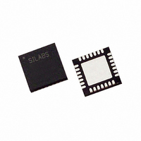
C8051F321-GMR Silicon Laboratories Inc, C8051F321-GMR Datasheet - Page 57

C8051F321-GMR
Manufacturer Part Number
C8051F321-GMR
Description
IC 8051 MCU 16K FLASH 28MLP
Manufacturer
Silicon Laboratories Inc
Series
C8051F32xr
Specifications of C8051F321-GMR
Core Processor
8051
Core Size
8-Bit
Speed
25MHz
Connectivity
SMBus (2-Wire/I²C), SPI, UART/USART, USB
Peripherals
Brown-out Detect/Reset, POR, PWM, Temp Sensor, WDT
Number Of I /o
21
Program Memory Size
16KB (16K x 8)
Program Memory Type
FLASH
Ram Size
2.25K x 8
Voltage - Supply (vcc/vdd)
2.7 V ~ 3.6 V
Data Converters
A/D 13x10b
Oscillator Type
Internal
Operating Temperature
-40°C ~ 85°C
Package / Case
28-VQFN Exposed Pad, 28-HVQFN, 28-SQFN, 28-DHVQFN
Processor Series
C8051F3x
Core
8051
Data Bus Width
8 bit
Data Ram Size
2.25 KB
Interface Type
I2C, SMBus, SPI, UART, USB
Maximum Clock Frequency
25 MHz
Number Of Programmable I/os
21
Number Of Timers
4
Maximum Operating Temperature
+ 85 C
Mounting Style
SMD/SMT
3rd Party Development Tools
PK51, CA51, A51, ULINK2
Development Tools By Supplier
C8051F320DK
Minimum Operating Temperature
- 40 C
On-chip Adc
10 bit, 13 Channel / 10 bit, 7 Channel
Package
28MLP
Device Core
8051
Family Name
C8051F321
Maximum Speed
25 MHz
Operating Supply Voltage
3.3 V
For Use With
336-1480 - DAUGHTER CARD TOOLSTCK C8051F321336-1449 - ADAPTER PROGRAM TOOLSTICK F321336-1260 - DEV KIT FOR C8051F320/F321
Lead Free Status / RoHS Status
Lead free / RoHS Compliant
Eeprom Size
-
Lead Free Status / Rohs Status
Details
Available stocks
Company
Part Number
Manufacturer
Quantity
Price
Part Number:
C8051F321-GMR
Manufacturer:
SILICON LABS/èٹ¯ç§‘
Quantity:
20 000
- Current page: 57 of 250
- Download datasheet (2Mb)
7.
C8051F320/1 devices include two on-chip programmable voltage Comparators: Comparator0 is shown in
Figure 7.1; Comparator1 is shown in Figure 7.2. The two Comparators operate identically with the follow-
ing exceptions: (1) Their input selections differ as shown in Figure 7.1 and Figure 7.2; (2) Comparator0 can
be used as a reset source.
Each Comparator offers programmable response time and hysteresis, an analog input multiplexer, and two
outputs that are optionally available at the Port pins: a synchronous “latched” output (CP0, CP1), or an
asynchronous “raw” output (CP0A, CP1A). The asynchronous signal is available even when the system
clock is not active. This allows the Comparators to operate and generate an output with the device in
STOP mode. When assigned to a Port pin, the Comparator outputs may be configured as open drain or
push-pull (see Section “14.2. Port I/O Initialization” on page 130). Comparator0 may also be used as a
reset source (see Section “10.5. Comparator0 Reset” on page 102).
The Comparator0 inputs are selected in the CPT0MX register (Figure 7.2). The CMX0P1–CMX0P0 bits
select the Comparator0 positive input; the CMX0N1–CMX0N0 bits select the Comparator0 negative input.
The Comparator1 inputs are selected in the CPT1MX register (Figure 7.5). The CMX1P1–CMX1P0 bits
select the Comparator1 positive input; the CMX1N1–CMX1N0 bits select the Comparator1 negative input.
Important Note About Comparator Inputs: The Port pins selected as Comparator inputs should be con-
figured as analog inputs in their associated Port configuration register, and configured to be skipped by the
Crossbar (for details on Port configuration, see Section “14.3. General Purpose Port I/O” on page 132).
Comparators
CMX0N1
CMX0N0
CMX0P1
CMX0P0
Note: P2.4 and P2.5 available
only on C8051F320
P1.0
P1.4
P2.0
P2.4
P1.1
P1.5
P2.1
P2.5
Figure 7.1. Comparator0 Functional Block Diagram
CP0HYP1
CP0HYP0
CP0HYN1
CP0HYN0
CP0OUT
CP0RIF
CP0FIF
CP0EN
CP0 +
CP0 -
CP0MD1
CP0MD0
CP0RIE
CP0FIE
Rev. 1.4
+
-
VDD
GND
Decision
Reset
Tree
(SYNCHRONIZER)
D
SET
CLR
Q
Q
D
SET
CLR
Q
Q
Rising-edge
CP0
C8051F320/1
Crossbar
Interrupt
Logic
Falling-edge
Interrupt
CP0
CP0A
CP0
CP0
CP0RIE
CP0FIE
57
Related parts for C8051F321-GMR
Image
Part Number
Description
Manufacturer
Datasheet
Request
R
Part Number:
Description:
SMD/C°/SINGLE-ENDED OUTPUT SILICON OSCILLATOR
Manufacturer:
Silicon Laboratories Inc
Part Number:
Description:
Manufacturer:
Silicon Laboratories Inc
Datasheet:
Part Number:
Description:
N/A N/A/SI4010 AES KEYFOB DEMO WITH LCD RX
Manufacturer:
Silicon Laboratories Inc
Datasheet:
Part Number:
Description:
N/A N/A/SI4010 SIMPLIFIED KEY FOB DEMO WITH LED RX
Manufacturer:
Silicon Laboratories Inc
Datasheet:
Part Number:
Description:
N/A/-40 TO 85 OC/EZLINK MODULE; F930/4432 HIGH BAND (REV E/B1)
Manufacturer:
Silicon Laboratories Inc
Part Number:
Description:
EZLink Module; F930/4432 Low Band (rev e/B1)
Manufacturer:
Silicon Laboratories Inc
Part Number:
Description:
I°/4460 10 DBM RADIO TEST CARD 434 MHZ
Manufacturer:
Silicon Laboratories Inc
Part Number:
Description:
I°/4461 14 DBM RADIO TEST CARD 868 MHZ
Manufacturer:
Silicon Laboratories Inc
Part Number:
Description:
I°/4463 20 DBM RFSWITCH RADIO TEST CARD 460 MHZ
Manufacturer:
Silicon Laboratories Inc
Part Number:
Description:
I°/4463 20 DBM RADIO TEST CARD 868 MHZ
Manufacturer:
Silicon Laboratories Inc
Part Number:
Description:
I°/4463 27 DBM RADIO TEST CARD 868 MHZ
Manufacturer:
Silicon Laboratories Inc
Part Number:
Description:
I°/4463 SKYWORKS 30 DBM RADIO TEST CARD 915 MHZ
Manufacturer:
Silicon Laboratories Inc
Part Number:
Description:
N/A N/A/-40 TO 85 OC/4463 RFMD 30 DBM RADIO TEST CARD 915 MHZ
Manufacturer:
Silicon Laboratories Inc
Part Number:
Description:
I°/4463 20 DBM RADIO TEST CARD 169 MHZ
Manufacturer:
Silicon Laboratories Inc


