MC9S12C32CFUE16 Freescale Semiconductor, MC9S12C32CFUE16 Datasheet - Page 290
MC9S12C32CFUE16
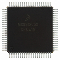
Manufacturer Part Number
MC9S12C32CFUE16
Description
IC MCU 32K FLASH 16MHZ 80-QFP
Manufacturer
Freescale Semiconductor
Series
HCS12r
Datasheets
1.MC9S12GC16MFUE.pdf
(690 pages)
2.MC9S12C96CFUER.pdf
(26 pages)
3.MC9S12C32CFAE25.pdf
(2 pages)
Specifications of MC9S12C32CFUE16
Core Processor
HCS12
Core Size
16-Bit
Speed
16MHz
Connectivity
CAN, EBI/EMI, SCI, SPI
Peripherals
POR, PWM, WDT
Number Of I /o
60
Program Memory Size
32KB (32K x 8)
Program Memory Type
FLASH
Ram Size
2K x 8
Voltage - Supply (vcc/vdd)
2.35 V ~ 5.5 V
Data Converters
A/D 8x10b
Oscillator Type
Internal
Operating Temperature
-40°C ~ 85°C
Package / Case
80-QFP
Processor Series
S12C
Core
HCS12
Data Bus Width
16 bit
Data Ram Size
2 KB
Interface Type
CAN/SCI/SPI
Maximum Clock Frequency
16 MHz
Number Of Programmable I/os
60
Number Of Timers
8
Operating Supply Voltage
- 0.3 V to + 6.5 V
Maximum Operating Temperature
+ 85 C
Mounting Style
SMD/SMT
3rd Party Development Tools
EWHCS12
Development Tools By Supplier
M68EVB912C32EE
Minimum Operating Temperature
- 40 C
On-chip Adc
8-ch x 10-bit
For Use With
CML12C32SLK - KIT STUDENT LEARNING 16BIT HCS12
Lead Free Status / RoHS Status
Lead free / RoHS Compliant
Eeprom Size
-
Lead Free Status / Rohs Status
Lead free / RoHS Compliant
Available stocks
Company
Part Number
Manufacturer
Quantity
Price

Company:
Part Number:
MC9S12C32CFUE16
Manufacturer:
Freescale Semiconductor
Quantity:
10 000


Chapter 10 Freescale’s Scalable Controller Area Network (S12MSCANV2)
10.3
Memory Map and Register Definition
This section provides a detailed description of all registers accessible in the MSCAN.
10.3.1
Module Memory Map
Figure 10-3
gives an overview on all registers and their individual bits in the MSCAN memory map. The
register address results from the addition of base address and address offset. The base address is
determined at the MCU level and can be found in the MCU memory map description. The address offset
is defined at the module level.
The MSCAN occupies 64 bytes in the memory space. The base address of the MSCAN module is
determined at the MCU level when the MCU is defined. The register decode map is fixed and begins at the
first address of the module address offset.
The detailed register descriptions follow in the order they appear in the register map.
290
MC9S12C-Family / MC9S12GC-Family
Freescale Semiconductor
Rev 01.24
Related parts for MC9S12C32CFUE16
Image
Part Number
Description
Manufacturer
Datasheet
Request
R

Part Number:
Description:
Manufacturer:
Freescale Semiconductor, Inc
Datasheet:
Part Number:
Description:
Manufacturer:
Freescale Semiconductor, Inc
Datasheet:
Part Number:
Description:
Manufacturer:
Freescale Semiconductor, Inc
Datasheet:
Part Number:
Description:
Manufacturer:
Freescale Semiconductor, Inc
Datasheet:
Part Number:
Description:
Manufacturer:
Freescale Semiconductor, Inc
Datasheet:
Part Number:
Description:
Manufacturer:
Freescale Semiconductor, Inc
Datasheet:
Part Number:
Description:
Manufacturer:
Freescale Semiconductor, Inc
Datasheet:
Part Number:
Description:
Manufacturer:
Freescale Semiconductor, Inc
Datasheet:
Part Number:
Description:
Manufacturer:
Freescale Semiconductor, Inc
Datasheet:
Part Number:
Description:
Manufacturer:
Freescale Semiconductor, Inc
Datasheet:
Part Number:
Description:
Manufacturer:
Freescale Semiconductor, Inc
Datasheet:
Part Number:
Description:
Manufacturer:
Freescale Semiconductor, Inc
Datasheet:
Part Number:
Description:
Manufacturer:
Freescale Semiconductor, Inc
Datasheet:
Part Number:
Description:
Manufacturer:
Freescale Semiconductor, Inc
Datasheet:
Part Number:
Description:
Manufacturer:
Freescale Semiconductor, Inc
Datasheet: