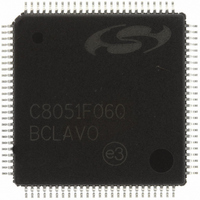
C8051F060-GQ Silicon Laboratories Inc, C8051F060-GQ Datasheet - Page 77

C8051F060-GQ
Manufacturer Part Number
C8051F060-GQ
Description
IC 8051 MCU 64K FLASH 100TQFP
Manufacturer
Silicon Laboratories Inc
Series
C8051F06xr
Specifications of C8051F060-GQ
Program Memory Type
FLASH
Program Memory Size
64KB (64K x 8)
Package / Case
100-TQFP, 100-VQFP
Core Processor
8051
Core Size
8-Bit
Speed
25MHz
Connectivity
CAN, EBI/EMI, SMBus (2-Wire/I²C), SPI, UART/USART
Peripherals
Brown-out Detect/Reset, POR, PWM, Temp Sensor, WDT
Number Of I /o
59
Ram Size
4.25K x 8
Voltage - Supply (vcc/vdd)
2.7 V ~ 3.6 V
Data Converters
A/D 2x16b, 8x10b; D/A 2x12b
Oscillator Type
Internal
Operating Temperature
-40°C ~ 85°C
Processor Series
C8051F0x
Core
8051
Data Bus Width
8 bit
Data Ram Size
4.25 KB
Interface Type
CAN/I2C/SMBus/SPI/UART
Maximum Clock Frequency
25 MHz
Number Of Programmable I/os
59
Number Of Timers
5
Operating Supply Voltage
2.7 V to 3.6 V
Maximum Operating Temperature
+ 85 C
Mounting Style
SMD/SMT
3rd Party Development Tools
PK51, CA51, A51, ULINK2
Development Tools By Supplier
C8051F060DK
Minimum Operating Temperature
- 40 C
On-chip Adc
8-ch x 10-bit
On-chip Dac
2-ch x 12-bit
No. Of I/o's
59
Ram Memory Size
4352Byte
Cpu Speed
25MHz
No. Of Timers
5
Rohs Compliant
Yes
Lead Free Status / RoHS Status
Lead free / RoHS Compliant
For Use With
336-1214 - DEV KIT FOR F060/F062/F063
Eeprom Size
-
Lead Free Status / Rohs Status
Lead free / RoHS Compliant
Other names
336-1213
Available stocks
Company
Part Number
Manufacturer
Quantity
Price
Company:
Part Number:
C8051F060-GQ
Manufacturer:
VISHAY
Quantity:
3 000
Company:
Part Number:
C8051F060-GQ
Manufacturer:
Silicon Laboratories Inc
Quantity:
10 000
Company:
Part Number:
C8051F060-GQR
Manufacturer:
Silicon Laboratories Inc
Quantity:
10 000
Company:
Part Number:
C8051F060-GQR.
Manufacturer:
SILICON
Quantity:
15 000
- Current page: 77 of 328
- Download datasheet (2Mb)
Pointer Registers are initialized to the values contained in the DMA Data Address Beginning Registers
(DMA0DAH and DMA0DAL). The Data Address Pointer Registers are automatically incremented by 2 or 4
after each data write by the DMA interface.
6.4.
When the DMA interface begins an operation cycle, the DMA Instruction Status Register (DMA0ISW,
Figure 6.9) is loaded with the address contained in the DMA Instruction Boundary Register (DMA0BND,
Figure 6.8). The instruction is fetched from the Instruction Buffer, and the DMA Control Logic waits for data
from the appropriate ADC(s). The DMA will execute each instruction once, and then increment DMA0ISW
to the next instruction address. When the current DMA instruction is an End of Operation instruction, the
Instruction Status Register is reset to the Instruction Boundary Register. If the Continuous Conversion bit
(bit 7, CCNV) in the End of Operation instruction word is set to ‘1’, the Repeat Counter is ignored, and the
DMA will continue to execute instructions indefinitely. When CCNV is set to ‘0’, the Repeat Counter (regis-
ters DMA0CSH and DMA0CSL) is decremented, and the DMA will continue to execute instructions until
the Repeat Counter reaches 0x0000. The Repeat Counter is initialized with the Repeat Counter Limit
value (registers DMA0CTH and DMA0CTL) at the beginning of the DMA operation. An example of Mode 0
operation is shown in Figure 6.2.
DMA0BND
Instruction Execution in Mode 0
0x3F
0x03
0x02
0x01
0x00
...
INSTRUCTION
(64 Bytes)
BUFFER
00000000
00110000
01000000
00010000
Figure 6.2. DMA Mode 0 Operation
Rev. 1.2
C8051F060/1/2/3/4/5/6/7
ADC0H (Diff.)
ADC0H (Diff.)
ADC0L (Diff.)
XRAM
ADC1H
ADC0H
ADC1H
ADC0H
ADC0H
ADC1L
ADC0L
ADC0L
ADC1L
ADC0L
ADC0L
DMA0CSH:L = 0x0000
DMA0CSH:L = DMA0CTH:L - 1
DMA0CSH:L = DMA0CTH:L
77
Related parts for C8051F060-GQ
Image
Part Number
Description
Manufacturer
Datasheet
Request
R
Part Number:
Description:
SMD/C°/SINGLE-ENDED OUTPUT SILICON OSCILLATOR
Manufacturer:
Silicon Laboratories Inc
Part Number:
Description:
Manufacturer:
Silicon Laboratories Inc
Datasheet:
Part Number:
Description:
N/A N/A/SI4010 AES KEYFOB DEMO WITH LCD RX
Manufacturer:
Silicon Laboratories Inc
Datasheet:
Part Number:
Description:
N/A N/A/SI4010 SIMPLIFIED KEY FOB DEMO WITH LED RX
Manufacturer:
Silicon Laboratories Inc
Datasheet:
Part Number:
Description:
N/A/-40 TO 85 OC/EZLINK MODULE; F930/4432 HIGH BAND (REV E/B1)
Manufacturer:
Silicon Laboratories Inc
Part Number:
Description:
EZLink Module; F930/4432 Low Band (rev e/B1)
Manufacturer:
Silicon Laboratories Inc
Part Number:
Description:
I°/4460 10 DBM RADIO TEST CARD 434 MHZ
Manufacturer:
Silicon Laboratories Inc
Part Number:
Description:
I°/4461 14 DBM RADIO TEST CARD 868 MHZ
Manufacturer:
Silicon Laboratories Inc
Part Number:
Description:
I°/4463 20 DBM RFSWITCH RADIO TEST CARD 460 MHZ
Manufacturer:
Silicon Laboratories Inc
Part Number:
Description:
I°/4463 20 DBM RADIO TEST CARD 868 MHZ
Manufacturer:
Silicon Laboratories Inc
Part Number:
Description:
I°/4463 27 DBM RADIO TEST CARD 868 MHZ
Manufacturer:
Silicon Laboratories Inc
Part Number:
Description:
I°/4463 SKYWORKS 30 DBM RADIO TEST CARD 915 MHZ
Manufacturer:
Silicon Laboratories Inc
Part Number:
Description:
N/A N/A/-40 TO 85 OC/4463 RFMD 30 DBM RADIO TEST CARD 915 MHZ
Manufacturer:
Silicon Laboratories Inc
Part Number:
Description:
I°/4463 20 DBM RADIO TEST CARD 169 MHZ
Manufacturer:
Silicon Laboratories Inc


