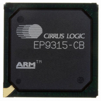
EP9315-CB Cirrus Logic Inc, EP9315-CB Datasheet - Page 60

EP9315-CB
Manufacturer Part Number
EP9315-CB
Description
IC ARM920T MCU 200MHZ 352-PBGA
Manufacturer
Cirrus Logic Inc
Series
EP9r
Specifications of EP9315-CB
Core Processor
ARM9
Core Size
16/32-Bit
Speed
200MHz
Connectivity
EBI/EMI, EIDE, Ethernet, I²C, IrDA, Keypad/Touchscreen, PCMCIA, SPI, UART/USART, USB
Peripherals
AC'97, DMA, I²:S, LCD, LED, MaverickKey, POR, PWM, WDT
Number Of I /o
16
Program Memory Type
ROMless
Ram Size
32K x 8
Voltage - Supply (vcc/vdd)
1.65 V ~ 3.6 V
Data Converters
A/D 8x12b
Oscillator Type
External
Operating Temperature
0°C ~ 70°C
Package / Case
352-BGA
Processor Series
EP93xx
Core
ARM920T
Data Bus Width
32 bit
3rd Party Development Tools
MDK-ARM, RL-ARM, ULINK2
Development Tools By Supplier
EDB9315A-Z
For Use With
598-1144 - KIT DEVELOPMENT EP9315 ARM9
Lead Free Status / RoHS Status
Contains lead / RoHS non-compliant
Eeprom Size
-
Program Memory Size
-
Lead Free Status / Rohs Status
No
Other names
598-1261
Available stocks
Company
Part Number
Manufacturer
Quantity
Price
Part Number:
EP9315-CBZ
Manufacturer:
CIRRUS
Quantity:
20 000
EP9315
Enhanced Universal Platform SOC Processor
The following section focuses on the EP9315 pin signals
from two viewpoints - the pin usage and pad
characteristics, and the pin multiplexing usage. The first
table
signals. The second table
signal multiplexing and configuration options.
Table S
illustrates the pad type and pad pull type (if any). The
symbols used in the table are defined as follows. (Note: A
blank box means Not Applicable (NA) or, for Pull Type,
No Pull (NP).)
.
60
TCK
TDI
TDO
TMS
TRSTn
BOOT[1:0]
XTALI
XTALO
VDD_PLL
GND_PLL
RTCXTALI
RTCXTALO
WRn
RDn
WAITn
AD[25:0]
DA[31:0]
CSn[3:0]
CSn[7:6]
DQMn[3:0]
SDCLK
SDCLKEN
SDCSn[3:0]
RASn
CASn
SDWEn
P[17:0]
Pin Name
(Table
is a summary of the EP9315 pin signals, which
SDRAM
SDRAM
SDRAM
SDRAM
SDRAM
SDRAM
System
Raster
Block
EBUS
EBUS
EBUS
EBUS
EBUS
EBUS
EBUS
EBUS
JTAG
JTAG
JTAG
JTAG
JTAG
RTC
RTC
PLL
PLL
PLL
PLL
S) is a summary of all the EP9315 pin
Table S. Pin Descriptions
Type
4ma
4ma
4ma
8ma
8ma
4ma
4ma
8ma
8ma
8ma
4ma
8ma
8ma
8ma
4ma
Pad
G
A
A
P
A
A
I
I
I
I
I
I
Type
Pull
PD
PD
PD
PD
PD
PU
PU
PU
PU
PU
(Table
JTAG clock in
JTAG data in
JTAG data out
JTAG test mode select
JTAG reset
Boot mode select in
Main oscillator input
Main oscillator output
Main oscillator power, 1.8V
Main oscillator ground
RTC oscillator input
RTC oscillator output
SRAM Write strobe out
SRAM Read / OE strobe out
SRAM Wait in
Shared Address bus out
Shared Data bus in/out
Chip select out
Chip select out
Shared data mask out
SDRAM clock out
SDRAM clock enable out
SDRAM chip selects out
SDRAM RAS out
SDRAM CAS out
SDRAM write enable out
Pixel data bus out
©
T) illustrates the pin
Copyright 2005 Cirrus Logic (All Rights Reserved)
Description
Under the Pad Type column:
•
•
•
•
•
•
•
•
See the text description for additional information about
bi-directional pins.
Under the Pull Type Column:
•
•
SPCLK
HSYNC
V_CSYNC
BLANK
BRIGHT
PWMOUT
Xp, Xm
Yp, Ym
sXp, sXm
sYp, sYm
VDD_ADC
GND_ADC
COL[7:0]
ROW[7:0]
USBp[2:0]
USBm[2:0]
TXD0
RXD0
CTSn
DSRn
DTRn
RTSn
TXD1
RXD1
TXD2
RXD2
MDC
Pin Name
A - Analog pad
P - Power pad
G - Ground pad
I - Pin is an input only
I/O - Pin is input/output
4mA - Pin is a 4 mA output driver
8mA - Pin is an 8 mA output driver
12mA - Pin is an 12 mA output driver
PU - Resistor is a pull up to the RVDD supply
PD - Resistor is a pull down to the RGND supply
UART1
UART1
UART1
UART1
UART1
UART1
UART2
UART2
UART3
UART3
Raster
Raster
Raster
Raster
Raster
EMAC
Block
PWM
ADC
ADC
ADC
ADC
ADC
ADC
USB
USB
Key
Key
Table S. Pin Descriptions (Continued)
12ma
Type
8ma
8ma
8ma
4ma
8ma
8ma
8ma
4ma
4ma
4ma
4ma
4ma
4ma
Pad
A
A
A
A
P
G
A
A
I
I
I
I
I
Type
Pull
PU
PU
PU
PU
PU
PU
PU
PU
PU
PU
PU
Pixel clock in/out
Horizontal synchronization / line pulse out
Vertical or composite synchronization / frame
pulse out
Composite blanking signal out
PWM brightness control out
Pulse width modulator output
Touchscreen ADC X axis
Touchscreen ADC Y axis
Touchscreen ADC X axis feedback
Touchscreen ADC Y axis feedback
Touchscreen ADC power, 3.3V
Touchscreen ADC ground
Key matrix column inputs
Key matrix row outputs
USB positive signals
USB negative signals
Transmit out
Receive in
Clear to send / transmit enable
Data set ready / Data Carrier Detect
Data Terminal Ready output
Ready to send
Transmit / IrDA output
Receive / IrDA input
Transmit
Receive
Management data clock
Description
DS638PP4


