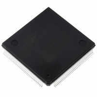
ST10F276Z5Q3TR STMicroelectronics, ST10F276Z5Q3TR Datasheet - Page 175

ST10F276Z5Q3TR
Manufacturer Part Number
ST10F276Z5Q3TR
Description
MCU 16BIT 832KBIT FLASH 144-PQFP
Manufacturer
STMicroelectronics
Series
ST10r
Datasheet
1.ST10F276Z5T3.pdf
(239 pages)
Specifications of ST10F276Z5Q3TR
Core Processor
ST10
Core Size
16-Bit
Speed
64MHz
Connectivity
ASC, CAN, EBI/EMI, I²C, SSC, UART/USART
Peripherals
POR, PWM, WDT
Number Of I /o
111
Program Memory Size
832KB (832K x 8)
Program Memory Type
FLASH
Ram Size
68K x 8
Voltage - Supply (vcc/vdd)
4.5 V ~ 5.5 V
Data Converters
A/D 24x10b
Oscillator Type
Internal
Operating Temperature
-40°C ~ 125°C
Package / Case
144-QFP
Processor Series
ST10F27x
Core
ST10
Data Bus Width
16 bit
Data Ram Size
68 KB
Interface Type
CAN, I2C
Maximum Clock Frequency
64 MHz
Number Of Programmable I/os
111
Number Of Timers
5
Maximum Operating Temperature
+ 125 C
Mounting Style
SMD/SMT
Minimum Operating Temperature
- 40 C
On-chip Adc
10 bit, 24 Channel
For Use With
497-6399 - KIT DEV STARTER ST10F276Z5
Lead Free Status / RoHS Status
Lead free / RoHS Compliant
Eeprom Size
-
Lead Free Status / Rohs Status
Details
Available stocks
Company
Part Number
Manufacturer
Quantity
Price
Company:
Part Number:
ST10F276Z5Q3TR
Manufacturer:
STMicroelectronics
Quantity:
10 000
- Current page: 175 of 239
- Download datasheet (3Mb)
ST10F276Z5
Table 86.
When CAN1, CAN2, RTC, XASC, XSSC, I
all disabled via XPERCON setting, then any access in the address range 00’E800h -
00’EFFFh is directed to external memory interface, using the BUSCONx register
corresponding to the address matching ADDRSELx register. All pins used for X-Peripherals
can be used as General Purpose I/O whenever the related module is not enabled.
XRTCEN
XPWMEN
XFLASHEN
XASCEN
XSSCEN
XI2CEN
XMISCEN
Bit
ESFR description (continued)
RTC enable
‘0’: Accesses to the on-chip RTC module are disabled, external access performed.
Address range 00’ED00h-00’EDFF is directed to external memory only if
CAN1EN, CAN2EN, XASCEN, XSSCEN, XI2CEN, XPWMEN and XMISCEN are
‘0’ also.
‘1’: The on-chip RTC module is enabled and can be accessed.
XPWM enable
‘0’: Accesses to the on-chip XPWM module are disabled, external access
performed. Address range 00’EC00h-00’ECFF is directed to external memory only
if CAN1EN, CAN2EN, XASCEN, XSSCEN, XI2CEN, XRTCEN and XMISCEN are
‘0’ also.
‘1’: The on-chip XPWM module is enabled and can be accessed.
XFlash enable bit
‘0’: Accesses to the on-chip XFlash and Flash registers are disabled, external
access performed. Address range 09’0000h-0E’FFFFh is directed to external
memory only if XRAM2EN is ‘0’ also.
‘1’: The on-chip XFlash is enabled and can be accessed.
XASC enable bit
‘0’: Accesses to the on-chip XASC are disabled, external access performed.
Address range 00’E900h-00’E9FFh is directed to external memory only if
CAN1EN, CAN2EN, XRTCEN, XASCEN, XI2CEN, XPWMEN and XMISCEN are
‘0’ also.
‘1’: The on-chip XASC is enabled and can be accessed.
XSSC enable bit
‘0’: Accesses to the on-chip XSSC are disabled, external access performed.
Address range 00’E800h-00’E8FFh is directed to external memory only if
CAN1EN, CAN2EN, XRTCEN, XASCEN, XI2CEN, XPWMEN and XMISCEN are
‘0’ also.
‘1’: The on-chip XSSC is enabled and can be accessed.
I
‘0’: Accesses to the on-chip I
range 00’EA00h-00’EAFFh is directed to external memory only if CAN1EN,
CAN2EN, XRTCEN, XASCEN, XSSCEN, XPWMEN and XMISCEN are ‘0’ also.
‘1’: The on-chip I
XBUS additional features enable bit
‘0’: Accesses to the Additional Miscellaneous Features is disabled. Address range
00’EB00h-00’EBFFh is directed to external memory only if CAN1EN, CAN2EN,
XRTCEN, XASCEN, XSSCEN, XPWMEN and XI2CEN are ‘0’ also.
‘1’: The Additional Features are enabled and can be accessed.
2
C enable bit
2
C is enabled and can be accessed.
2
2
C, XPWM and the XBUS Additional Features are
C are disabled, external access performed. Address
Function
Register set
175/239
Related parts for ST10F276Z5Q3TR
Image
Part Number
Description
Manufacturer
Datasheet
Request
R

Part Number:
Description:
MCU 16BIT 832K FLASH 144-LQFP
Manufacturer:
STMicroelectronics
Datasheet:

Part Number:
Description:
MCU 16BIT 832K FLASH 144-LQFP
Manufacturer:
STMicroelectronics
Datasheet:

Part Number:
Description:
MCU 16BIT 832K FLASH 144-PQFP
Manufacturer:
STMicroelectronics
Datasheet:

Part Number:
Description:
MCU 16BIT 832K FLASH 144-PQFP
Manufacturer:
STMicroelectronics
Datasheet:

Part Number:
Description:
16-bit Microcontrollers - MCU 16-Bit MCU 832 kByte 68 KB RAM CMOS
Manufacturer:
STMicroelectronics

Part Number:
Description:
STMicroelectronics [RIPPLE-CARRY BINARY COUNTER/DIVIDERS]
Manufacturer:
STMicroelectronics
Datasheet:

Part Number:
Description:
STMicroelectronics [LIQUID-CRYSTAL DISPLAY DRIVERS]
Manufacturer:
STMicroelectronics
Datasheet:

Part Number:
Description:
BOARD EVAL FOR MEMS SENSORS
Manufacturer:
STMicroelectronics
Datasheet:

Part Number:
Description:
NPN TRANSISTOR POWER MODULE
Manufacturer:
STMicroelectronics
Datasheet:

Part Number:
Description:
TURBOSWITCH ULTRA-FAST HIGH VOLTAGE DIODE
Manufacturer:
STMicroelectronics
Datasheet:

Part Number:
Description:
Manufacturer:
STMicroelectronics
Datasheet:

Part Number:
Description:
DIODE / SCR MODULE
Manufacturer:
STMicroelectronics
Datasheet:


