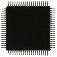
MC9S12C96CFUE Freescale Semiconductor, MC9S12C96CFUE Datasheet - Page 183

MC9S12C96CFUE
Manufacturer Part Number
MC9S12C96CFUE
Description
IC MCU 96K FLASH 4K RAM 80-QFP
Manufacturer
Freescale Semiconductor
Series
HCS12r
Specifications of MC9S12C96CFUE
Core Processor
HCS12
Core Size
16-Bit
Speed
25MHz
Connectivity
CAN, EBI/EMI, SCI, SPI
Peripherals
POR, PWM, WDT
Number Of I /o
60
Program Memory Size
96KB (96K x 8)
Program Memory Type
FLASH
Ram Size
4K x 8
Voltage - Supply (vcc/vdd)
2.35 V ~ 5.5 V
Data Converters
A/D 8x10b
Oscillator Type
Internal
Operating Temperature
-40°C ~ 85°C
Package / Case
80-QFP
Processor Series
S12C
Core
HCS12
Data Bus Width
16 bit
Data Ram Size
4 KB
Interface Type
CAN/SCI/SPI
Maximum Clock Frequency
25 MHz
Number Of Programmable I/os
60
Number Of Timers
8
Operating Supply Voltage
- 0.3 V to + 6.5 V
Maximum Operating Temperature
+ 85 C
Mounting Style
SMD/SMT
3rd Party Development Tools
EWHCS12
Development Tools By Supplier
M68EVB912C32EE
Minimum Operating Temperature
- 40 C
On-chip Adc
8-ch x 10-bit
Lead Free Status / RoHS Status
Lead free / RoHS Compliant
Eeprom Size
-
Lead Free Status / Rohs Status
Lead free / RoHS Compliant
Available stocks
Company
Part Number
Manufacturer
Quantity
Price
Company:
Part Number:
MC9S12C96CFUE
Manufacturer:
Freescale Semiconductor
Quantity:
10 000
Company:
Part Number:
MC9S12C96CFUER
Manufacturer:
Freescale Semiconductor
Quantity:
10 000
- Current page: 183 of 690
- Download datasheet (4Mb)
Figure 6-11
instruction is used as an example. First, the 8-bit instruction opcode is sent by the host, followed by the
address of the memory location to be read. The target BDM decodes the instruction. A bus cycle is grabbed
(free or stolen) by the BDM and it executes the READ_BYTE operation. Having retrieved the data, the
BDM issues an ACK pulse to the host controller, indicating that the addressed byte is ready to be retrieved.
After detecting the ACK pulse, the host initiates the byte retrieval process. Note that data is sent in the form
of a word and the host needs to determine which is the appropriate byte based on whether the address was
odd or even.
Differently from the normal bit transfer (where the host initiates the transmission), the serial interface ACK
handshake pulse is initiated by the target MCU by issuing a falling edge in the BKGD pin. The hardware
handshake protocol in
should follow this timing constraint in order to avoid the risk of an electrical conflict in the BKGD pin.
The ACK handshake protocol does not support nested ACK pulses. If a BDM command is not
acknowledge by an ACK pulse, the host needs to abort the pending command first in order to be able to
issue a new BDM command. When the CPU enters WAIT or STOP while the host issues a command that
requires CPU execution (e.g., WRITE_BYTE), the target discards the incoming command due to the
WAIT or STOP being detected. Therefore, the command is not acknowledged by the target, which means
that the ACK pulse will not be issued in this case. After a certain time the host should decide to abort the
ACK sequence in order to be free to issue a new command. Therefore, the protocol should provide a
mechanism in which a command, and therefore a pending ACK, could be aborted.
Freescale Semiconductor
BKGD PIN
shows the ACK handshake protocol in a command level timing diagram. The READ_BYTE
READ_BYTE
The only place the BKGD pin can have an electrical conflict is when one
side is driving low and the other side is issuing a speedup pulse (high). Other
“highs” are pulled rather than driven. However, at low rates the time of the
speedup pulse can become lengthy and so the potential conflict time
becomes longer as well.
Differently from a regular BDM command, the ACK pulse does not provide
a time out. This means that in the case of a WAIT or STOP instruction being
executed, the ACK would be prevented from being issued. If not aborted, the
ACK would remain pending indefinitely. See the handshake abort procedure
described in
HOST
Figure 6-10
Figure 6-11. Handshake Protocol at Command Level
Section 6.4.8, “Hardware Handshake Abort
BYTE ADDRESS
TARGET
THE COMMAND
BDM DECODES
specifies the timing when the BKGD pin is being driven, so the host
MC9S12C-Family / MC9S12GC-Family
Rev 01.24
NOTE
NOTE
Chapter 6 Background Debug Module (BDMV4) Block Description
BDM EXECUTES THE
READ_BYTE COMMAND
TARGET
BDM ISSUES THE
ACK PULSE (OUT OF SCALE)
(2) BYTES ARE
RETRIEVED
Procedure.”
HOST
HOST
COMMAND
NEW BDM
TARGET
183
Related parts for MC9S12C96CFUE
Image
Part Number
Description
Manufacturer
Datasheet
Request
R
Part Number:
Description:
Manufacturer:
Freescale Semiconductor, Inc
Datasheet:
Part Number:
Description:
Manufacturer:
Freescale Semiconductor, Inc
Datasheet:
Part Number:
Description:
Manufacturer:
Freescale Semiconductor, Inc
Datasheet:
Part Number:
Description:
Manufacturer:
Freescale Semiconductor, Inc
Datasheet:
Part Number:
Description:
Manufacturer:
Freescale Semiconductor, Inc
Datasheet:
Part Number:
Description:
Manufacturer:
Freescale Semiconductor, Inc
Datasheet:
Part Number:
Description:
Manufacturer:
Freescale Semiconductor, Inc
Datasheet:
Part Number:
Description:
Manufacturer:
Freescale Semiconductor, Inc
Datasheet:
Part Number:
Description:
Manufacturer:
Freescale Semiconductor, Inc
Datasheet:
Part Number:
Description:
Manufacturer:
Freescale Semiconductor, Inc
Datasheet:
Part Number:
Description:
Manufacturer:
Freescale Semiconductor, Inc
Datasheet:
Part Number:
Description:
Manufacturer:
Freescale Semiconductor, Inc
Datasheet:
Part Number:
Description:
Manufacturer:
Freescale Semiconductor, Inc
Datasheet:
Part Number:
Description:
Manufacturer:
Freescale Semiconductor, Inc
Datasheet:
Part Number:
Description:
Manufacturer:
Freescale Semiconductor, Inc
Datasheet:


