MC9S12C96CFUE Freescale Semiconductor, MC9S12C96CFUE Datasheet - Page 438
MC9S12C96CFUE
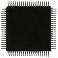
Manufacturer Part Number
MC9S12C96CFUE
Description
IC MCU 96K FLASH 4K RAM 80-QFP
Manufacturer
Freescale Semiconductor
Series
HCS12r
Specifications of MC9S12C96CFUE
Core Processor
HCS12
Core Size
16-Bit
Speed
25MHz
Connectivity
CAN, EBI/EMI, SCI, SPI
Peripherals
POR, PWM, WDT
Number Of I /o
60
Program Memory Size
96KB (96K x 8)
Program Memory Type
FLASH
Ram Size
4K x 8
Voltage - Supply (vcc/vdd)
2.35 V ~ 5.5 V
Data Converters
A/D 8x10b
Oscillator Type
Internal
Operating Temperature
-40°C ~ 85°C
Package / Case
80-QFP
Processor Series
S12C
Core
HCS12
Data Bus Width
16 bit
Data Ram Size
4 KB
Interface Type
CAN/SCI/SPI
Maximum Clock Frequency
25 MHz
Number Of Programmable I/os
60
Number Of Timers
8
Operating Supply Voltage
- 0.3 V to + 6.5 V
Maximum Operating Temperature
+ 85 C
Mounting Style
SMD/SMT
3rd Party Development Tools
EWHCS12
Development Tools By Supplier
M68EVB912C32EE
Minimum Operating Temperature
- 40 C
On-chip Adc
8-ch x 10-bit
Lead Free Status / RoHS Status
Lead free / RoHS Compliant
Eeprom Size
-
Lead Free Status / Rohs Status
Lead free / RoHS Compliant
Available stocks
Company
Part Number
Manufacturer
Quantity
Price

Company:
Part Number:
MC9S12C96CFUE
Manufacturer:
Freescale Semiconductor
Quantity:
10 000
Company:
Part Number:
MC9S12C96CFUER
Manufacturer:
Freescale Semiconductor
Quantity:
10 000


Chapter 15 Timer Module (TIM16B8CV1) Block Description
15.2
The TIM16B8CV1 module has a total of eight external pins.
15.2.1
This pin serves as input capture or output compare for channel 7. This can also be configured as pulse
accumulator input.
15.2.2
This pin serves as input capture or output compare for channel 6.
15.2.3
This pin serves as input capture or output compare for channel 5.
15.2.4
This pin serves as input capture or output compare for channel 4. Pin
15.2.5
This pin serves as input capture or output compare for channel 3.
438
External Signal Description
IOC7 — Input Capture and Output Compare Channel 7 Pin
IOC6 — Input Capture and Output Compare Channel 6 Pin
IOC5 — Input Capture and Output Compare Channel 5 Pin
IOC4 — Input Capture and Output Compare Channel 4 Pin
IOC3 — Input Capture and Output Compare Channel 3 Pin
For more information see the respective functional descriptions in
Section 15.4, “Functional Description,”
CHANNEL 7 OUTPUT COMPARE
Figure 15-4. Channel 7 Output Compare/Pulse Accumulator Logic
PULSE
ACCUMULATOR
OC7M7
OM7
OL7
MC9S12C-Family / MC9S12GC-Family
Rev 01.24
NOTE
of this document.
PAD
Freescale Semiconductor
Related parts for MC9S12C96CFUE
Image
Part Number
Description
Manufacturer
Datasheet
Request
R

Part Number:
Description:
Manufacturer:
Freescale Semiconductor, Inc
Datasheet:
Part Number:
Description:
Manufacturer:
Freescale Semiconductor, Inc
Datasheet:
Part Number:
Description:
Manufacturer:
Freescale Semiconductor, Inc
Datasheet:
Part Number:
Description:
Manufacturer:
Freescale Semiconductor, Inc
Datasheet:
Part Number:
Description:
Manufacturer:
Freescale Semiconductor, Inc
Datasheet:
Part Number:
Description:
Manufacturer:
Freescale Semiconductor, Inc
Datasheet:
Part Number:
Description:
Manufacturer:
Freescale Semiconductor, Inc
Datasheet:
Part Number:
Description:
Manufacturer:
Freescale Semiconductor, Inc
Datasheet:
Part Number:
Description:
Manufacturer:
Freescale Semiconductor, Inc
Datasheet:
Part Number:
Description:
Manufacturer:
Freescale Semiconductor, Inc
Datasheet:
Part Number:
Description:
Manufacturer:
Freescale Semiconductor, Inc
Datasheet:
Part Number:
Description:
Manufacturer:
Freescale Semiconductor, Inc
Datasheet:
Part Number:
Description:
Manufacturer:
Freescale Semiconductor, Inc
Datasheet:
Part Number:
Description:
Manufacturer:
Freescale Semiconductor, Inc
Datasheet:
Part Number:
Description:
Manufacturer:
Freescale Semiconductor, Inc
Datasheet: