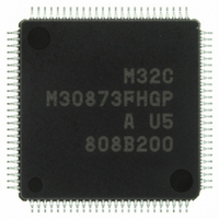
M30873FHGP#U5 Renesas Electronics America, M30873FHGP#U5 Datasheet - Page 152

M30873FHGP#U5
Manufacturer Part Number
M30873FHGP#U5
Description
IC M32C/87 MCU FLASH 100LQFP
Manufacturer
Renesas Electronics America
Series
M16C™ M32C/80r
Datasheet
1.M3087BFLGPU3.pdf
(629 pages)
Specifications of M30873FHGP#U5
Core Processor
M32C/80
Core Size
16/32-Bit
Speed
32MHz
Connectivity
CAN, EBI/EMI, I²C, IEBus, IrDA, SIO, UART/USART
Peripherals
DMA, POR, PWM, WDT
Number Of I /o
85
Program Memory Size
384KB (384K x 8)
Program Memory Type
FLASH
Ram Size
24K x 8
Voltage - Supply (vcc/vdd)
3 V ~ 5.5 V
Data Converters
A/D 26x10b; D/A 2x8b
Oscillator Type
Internal
Operating Temperature
-20°C ~ 85°C
Package / Case
100-LQFP
For Use With
R0K330879S001BE - KIT DEV RSK M32C/87R0K330879S000BE - KIT DEV RSK M32C/87
Lead Free Status / RoHS Status
Lead free / RoHS Compliant
Eeprom Size
-
Available stocks
Company
Part Number
Manufacturer
Quantity
Price
Part Number:
M30873FHGP#U5M30873FHGP#U3
Manufacturer:
Renesas Electronics America
Quantity:
10 000
- Current page: 152 of 629
- Download datasheet (16Mb)
M32C/87 Group (M32C/87, M32C/87A, M32C/87B)
REJ09B0180-0151 Rev.1.51 Jul 31, 2008
Page 128 of 587
11.11 Intelligent I/O Interrupts, CAN Interrupts, UART5 and UART6 Transmit/
Figure 11.17
The intelligent I/O interrupts are shared by CAN interrupt, INT6 to INT8 interrupts, UART5 and UART6 transmit/
receive interrupt. A logical sum of interrupt request signals from individual peripheral functions is used to generate
an interrupt.
Figure 11.17 shows a block diagram of the intelligent I/O interrupts. Figure 11.18 shows the IIOiIR (i = 0 to 11)
register. Figure 11.19 shows the IIOiIE register.
Interrupt request
Interrupt request
Interrupt request
"0" write signal
"0" write signal
"0" write signal
i = 0 to 11, j = 0 to 5
NOTES:
Receive Interrupts, and INT6 to INT8 Interrupts
1. Bits 1 to 7 in the IIOiIR register do not automatically become 0 when the interrupt request is acknowledged. Set to 0 by
2. Do not change the interrupt enable bit (bits 1 to 7 in the IIOiIE register) and IRLT bit in the IIOiIE register simultaneously.
to bit 1
to bit2
to bit7
signal
signal
signal
a program.
Intelligent I/O Interrupt Block Diagram
IIOiIE register
IIOiIR register
IRLT
bit 1
bit 2
bit 7
bit 1
bit 2
bit 7
S Q
R
S Q
R
S Q
R
(2)
(1)
0
1
0
1
0
1
When this signal changes from
0 to 1, the IR bit in the IIOiIC
(CANjIC) register becomes 1.
IR bit in the IIOiIC
(CANjIC) register
D Q
R
IR bit is cleared to 0 by an interrupt
request acknowledgement or by
writing a 0 to the IR bit.
To the interrupt priority
level decision circuit
11. Interrupts
Related parts for M30873FHGP#U5
Image
Part Number
Description
Manufacturer
Datasheet
Request
R

Part Number:
Description:
KIT STARTER FOR M16C/29
Manufacturer:
Renesas Electronics America
Datasheet:

Part Number:
Description:
KIT STARTER FOR R8C/2D
Manufacturer:
Renesas Electronics America
Datasheet:

Part Number:
Description:
R0K33062P STARTER KIT
Manufacturer:
Renesas Electronics America
Datasheet:

Part Number:
Description:
KIT STARTER FOR R8C/23 E8A
Manufacturer:
Renesas Electronics America
Datasheet:

Part Number:
Description:
KIT STARTER FOR R8C/25
Manufacturer:
Renesas Electronics America
Datasheet:

Part Number:
Description:
KIT STARTER H8S2456 SHARPE DSPLY
Manufacturer:
Renesas Electronics America
Datasheet:

Part Number:
Description:
KIT STARTER FOR R8C38C
Manufacturer:
Renesas Electronics America
Datasheet:

Part Number:
Description:
KIT STARTER FOR R8C35C
Manufacturer:
Renesas Electronics America
Datasheet:

Part Number:
Description:
KIT STARTER FOR R8CL3AC+LCD APPS
Manufacturer:
Renesas Electronics America
Datasheet:

Part Number:
Description:
KIT STARTER FOR RX610
Manufacturer:
Renesas Electronics America
Datasheet:

Part Number:
Description:
KIT STARTER FOR R32C/118
Manufacturer:
Renesas Electronics America
Datasheet:

Part Number:
Description:
KIT DEV RSK-R8C/26-29
Manufacturer:
Renesas Electronics America
Datasheet:

Part Number:
Description:
KIT STARTER FOR SH7124
Manufacturer:
Renesas Electronics America
Datasheet:

Part Number:
Description:
KIT STARTER FOR H8SX/1622
Manufacturer:
Renesas Electronics America
Datasheet:

Part Number:
Description:
KIT DEV FOR SH7203
Manufacturer:
Renesas Electronics America
Datasheet:


