M30873FHGP#U5 Renesas Electronics America, M30873FHGP#U5 Datasheet - Page 598
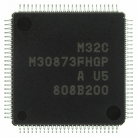
M30873FHGP#U5
Manufacturer Part Number
M30873FHGP#U5
Description
IC M32C/87 MCU FLASH 100LQFP
Manufacturer
Renesas Electronics America
Series
M16C™ M32C/80r
Datasheet
1.M3087BFLGPU3.pdf
(629 pages)
Specifications of M30873FHGP#U5
Core Processor
M32C/80
Core Size
16/32-Bit
Speed
32MHz
Connectivity
CAN, EBI/EMI, I²C, IEBus, IrDA, SIO, UART/USART
Peripherals
DMA, POR, PWM, WDT
Number Of I /o
85
Program Memory Size
384KB (384K x 8)
Program Memory Type
FLASH
Ram Size
24K x 8
Voltage - Supply (vcc/vdd)
3 V ~ 5.5 V
Data Converters
A/D 26x10b; D/A 2x8b
Oscillator Type
Internal
Operating Temperature
-20°C ~ 85°C
Package / Case
100-LQFP
For Use With
R0K330879S001BE - KIT DEV RSK M32C/87R0K330879S000BE - KIT DEV RSK M32C/87
Lead Free Status / RoHS Status
Lead free / RoHS Compliant
Eeprom Size
-
Available stocks
Company
Part Number
Manufacturer
Quantity
Price

Part Number:
M30873FHGP#U5M30873FHGP#U3
Manufacturer:
Renesas Electronics America
Quantity:
10 000


M32C/87 Group (M32C/87, M32C/87A, M32C/87B)
REJ09B0180-0151 Rev.1.51 Jul 31, 2008
Page 574 of 587
28.12 A/D Converter
Figure 28.5
•
•
•
•
•
•
•
•
To prevent latch-up and malfunction due to noise and also to minimize a conversion error, insert a capacitor
Set the ADST bit to 1 (A/D conversion starts) after setting registers AD0CON0 (ADST bit excluded),
AD0CON1, AD0CON2, AD0CON3, and AD0CON4.
When the VCUT bit in the AD0CON1 register is changed from 0 (VREF not connected) to 1 (VREF
connected), wait for 1 μs or more to start A/D conversion.
Set the VCUT bit to 0 when A/D conversion is not used to reduce current consumption.
between the AVSS pin and each of the following pins: the AVCC pin, VREF pin, or analog input pin ANi_j
(i = none, 0, 2, 15; j = 0 to 7). Insert a capacitor between the VCC pin and the VSS pin as well. Figure 28.5
shows an example of individual pin handling.
Set the port direction bit in the PDk register (k = 0 to 15), which corresponds to a pin used as an analog input
pin, to 0 (input mode). Also, set the port direction bit in the PDk register corresponding to the ADTRG pin, to
0 (input mode.)
When the key input interrupt is used, do not select pins P10_4 to P10_7 (AN_4 to AN_7) as analog input pins.
φAD frequency must be 16 MHz or lower when VCC1 = 4.2 V to 5.5 V, or 10 MHz or lower when
VCC1 = 3.0 V to 5.5 V. When the sample and hold is not activated, φAD frequency must be 250 kHz or higher.
When the sample and hold is activated, φAD frequency must be 1 MHz or higher.
When A/D operating mode is changed, set bits CH2 to CH0 in the AD0CON0 register or bits SCAN1 and
SCAN0 in the AD0CON1 register again to select analog input pins.
The voltage applied to AN_0 to AN_7, AN15_0 to AN15_7, ANEX0, and ANEX1 must be VCC1 or below.
The voltage applied to AN0_0 to AN0_7, and AN2_0 to AN2_7 must be VCC2 or below.
Individual Pin Handling
NOTES:
1. C1 ≥ 0.47 μ F, C2 ≥ 0.47 μ F, C3 ≥ 10000 pF, C4 ≥ 0.1 μ F, C5 ≥ 0.1 μ F (reference values)
2. Use thick and shortest possible wiring to connect capacitors.
VCC1
VCC2
C4
C5
VCC1
VSS
VCC2
VSS
MCU
AVCC
VREF
AVSS
ANi
C1
VCC1
C3
C2
28. Usage Notes
Related parts for M30873FHGP#U5
Image
Part Number
Description
Manufacturer
Datasheet
Request
R

Part Number:
Description:
KIT STARTER FOR M16C/29
Manufacturer:
Renesas Electronics America
Datasheet:

Part Number:
Description:
KIT STARTER FOR R8C/2D
Manufacturer:
Renesas Electronics America
Datasheet:

Part Number:
Description:
R0K33062P STARTER KIT
Manufacturer:
Renesas Electronics America
Datasheet:

Part Number:
Description:
KIT STARTER FOR R8C/23 E8A
Manufacturer:
Renesas Electronics America
Datasheet:

Part Number:
Description:
KIT STARTER FOR R8C/25
Manufacturer:
Renesas Electronics America
Datasheet:

Part Number:
Description:
KIT STARTER H8S2456 SHARPE DSPLY
Manufacturer:
Renesas Electronics America
Datasheet:

Part Number:
Description:
KIT STARTER FOR R8C38C
Manufacturer:
Renesas Electronics America
Datasheet:

Part Number:
Description:
KIT STARTER FOR R8C35C
Manufacturer:
Renesas Electronics America
Datasheet:

Part Number:
Description:
KIT STARTER FOR R8CL3AC+LCD APPS
Manufacturer:
Renesas Electronics America
Datasheet:
Part Number:
Description:
KIT STARTER FOR RX610
Manufacturer:
Renesas Electronics America
Datasheet:

Part Number:
Description:
KIT STARTER FOR R32C/118
Manufacturer:
Renesas Electronics America
Datasheet:

Part Number:
Description:
KIT DEV RSK-R8C/26-29
Manufacturer:
Renesas Electronics America
Datasheet:

Part Number:
Description:
KIT STARTER FOR SH7124
Manufacturer:
Renesas Electronics America
Datasheet:

Part Number:
Description:
KIT STARTER FOR H8SX/1622
Manufacturer:
Renesas Electronics America
Datasheet:

Part Number:
Description:
KIT DEV FOR SH7203
Manufacturer:
Renesas Electronics America
Datasheet: