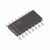
MAX791CSE+ Maxim Integrated Products, MAX791CSE+ Datasheet - Page 10

MAX791CSE+
Manufacturer Part Number
MAX791CSE+
Description
IC MPU SUPERVISOR CIRCUIT 16SOIC
Manufacturer
Maxim Integrated Products
Type
Battery Backup Circuitr
Datasheet
1.MAX791CSE.pdf
(19 pages)
Specifications of MAX791CSE+
Number Of Voltages Monitored
1
Output
Push-Pull, Totem Pole
Reset
Active Low
Reset Timeout
140 ms Minimum
Voltage - Threshold
4.65V
Operating Temperature
0°C ~ 70°C
Mounting Type
Surface Mount
Package / Case
16-SOIC (3.9mm Width)
Monitored Voltage
4.65 V
Undervoltage Threshold
4.5 V
Overvoltage Threshold
4.75 V
Manual Reset
Resettable
Watchdog
Yes
Battery Backup Switching
Yes
Power-up Reset Delay (typ)
280 ms
Supply Voltage (max)
5.5 V
Supply Voltage (min)
0 V
Supply Current (typ)
150 uA
Maximum Power Dissipation
696 mW
Mounting Style
SMD/SMT
Maximum Operating Temperature
+ 70 C
Chip Enable Signals
Yes
Minimum Operating Temperature
0 C
Output Type
Active Low or Open Drain or Push-Pull
Power Fail Detection
Yes
Lead Free Status / RoHS Status
Lead free / RoHS Compliant
As described in the preceding section, WDPO can be
used as the clock input to an external D flip-flop. Upon
the absence of a watchdog edge or pulse at WDI at the
end of a watchdog-timeout period, WDPO will pulse low
for 1ms. The falling edge of WDPO precedes WDO by
70ns. Since WDO is high when WDPO goes low, the
flip-flop’s Q output remains high as WDO goes low
(Figure 5). If the watchdog timer is not reset by a transi-
tion at WDI, WDO remains low and WDPO clocks a
logic low to the Q output, causing the MAX791 to latch
in reset. If the watchdog timer is reset by a transition at
WDI, WDO goes high and the flip-flop’s Q output
remains high. Thus, a system shutdown is only caused
by two successive watchdog faults.
The internal pull-up resistors associated with WDO and
WDPO connect to V
these outputs directly to CMOS logic that is powered
from V
mode), excessive current will flow from WDO or
WDPO through the protection diode(s) of the CMOS-
logic inputs to ground.
SWT input controls the watchdog-timeout period.
Connecting SWT to V
Microprocessor Supervisory Circuit
Figure 6. Two Consecutive Watchdog Faults Latch the System in Reset
10
______________________________________________________________________________________
CC
Selecting an Alternative Watchdog-
since, in the absence of V
REACTIVATE
*SETS Q HIGH ON POWER-UP
OUT
+5V
+5V
OUT
Watchdog-Pulse Output
selects the internal 1.6s watch-
. Therefore, do not connect
*1µF
3.6V
Timeout Period
CC
4.7k
(i.e., battery
1
9
VBATT
MR
MAX791
GND
V
4
LOWLINE
CC
3
RESET
WDPO
V
WDO
WDI
OUT
2
15
11
16
14
10
dog-timeout period. Select an alternative timeout period
by connecting a capacitor between SWT and GND. Do
not leave SWT floating, and do not connect it to ground.
The following formula determines the watchdog-timeout
period:
This formula is valid for capacitance values between
4.7nF and 100nF (see the Watchdog Timeout vs.
Timing Capacitor graph in the Typical Operating
Characteristics). SWT is internally connected to a
±100nA (typ) current source, which charges and dis-
charges the timing capacitor to create the oscillator fre-
quency that sets the watchdog-timeout period (see
Connecting a Timing Capacitor to SWT section).
The MAX791 provides internal gating of chip-enable
(CE) signals to prevent erroneous data from corrupting
the CMOS RAM in the event of a power failure. During
normal operation, the CE gate is enabled and passes
all CE transitions. When reset is asserted, this path
becomes disabled, preventing erroneous data from
corrupting the CMOS RAM. The MAX791 uses a series
transmission gate from the Chip-Enable Input (CE IN) to
CE OUT (Figure 1).
The 10ns max CE propagation from CE IN to CE OUT
1/6 74HC04
5
D
0.1µF
Watchdog-timeout period = 2.1 x (capacitor value
in nF) ms
CLOCK
SET
3
6
CD4013
RESET V
V
CC
4
14
SS
7
Q
Q
1
2
Chip-Enable Signal Gating
RESET
I/O
NMI
INTERRUPT
µP POWER
CONSECUTIVE
INDICATIONS
WATCHDOG
µP
FAULT
TWO


