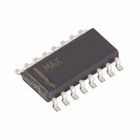
MAX791CSE+ Maxim Integrated Products, MAX791CSE+ Datasheet - Page 14

MAX791CSE+
Manufacturer Part Number
MAX791CSE+
Description
IC MPU SUPERVISOR CIRCUIT 16SOIC
Manufacturer
Maxim Integrated Products
Type
Battery Backup Circuitr
Datasheet
1.MAX791CSE.pdf
(19 pages)
Specifications of MAX791CSE+
Number Of Voltages Monitored
1
Output
Push-Pull, Totem Pole
Reset
Active Low
Reset Timeout
140 ms Minimum
Voltage - Threshold
4.65V
Operating Temperature
0°C ~ 70°C
Mounting Type
Surface Mount
Package / Case
16-SOIC (3.9mm Width)
Monitored Voltage
4.65 V
Undervoltage Threshold
4.5 V
Overvoltage Threshold
4.75 V
Manual Reset
Resettable
Watchdog
Yes
Battery Backup Switching
Yes
Power-up Reset Delay (typ)
280 ms
Supply Voltage (max)
5.5 V
Supply Voltage (min)
0 V
Supply Current (typ)
150 uA
Maximum Power Dissipation
696 mW
Mounting Style
SMD/SMT
Maximum Operating Temperature
+ 70 C
Chip Enable Signals
Yes
Minimum Operating Temperature
0 C
Output Type
Active Low or Open Drain or Push-Pull
Power Fail Detection
Yes
Lead Free Status / RoHS Status
Lead free / RoHS Compliant
The MAX791 is not short-circuit protected. Shorting
V
as charging a decoupling capacitor, destroys the
device.
All open-circuit outputs swing between V
rather than V
If long leads connect to the chip inputs, ensure that
these lines are free from ringing and other conditions
that would forward bias the chip’s protection diodes.
There are three distinct modes of operation:
VBATT has the same operating voltage range as V
and the battery-switchover threshold voltages are typi-
Microprocessor Supervisory Circuit
Figure 12. SuperCap or MaxCap on VBATT
14
1) Normal operating mode with all circuitry powered
2) Battery-backup mode where V
3) Battery-backup mode where V
OUT
______________________________________________________________________________________
up. Typical supply current from V
only leakage currents flow from the battery.
0.7V below VBATT. All circuitry is powered up and
the supply current from the battery is typically less
than 60µA.
VBATT by at least 0.7V. VBATT supply current is
less than 1µA max.
to ground, other than power-up transients such
+5V
1N4148
0.47F
CC
Applications Information
and GND.
Using SuperCaps or MaxCaps
1
VBATT
MAX791
GND
V
CC
3
4
with the MAX791
V
OUT
CC
CC
2
is typically within
CC
OUT
is 60µA, while
is less than
and GND
CC
,
cally ±30mV centered at VBATT, allowing use of a
SuperCap and a simple charging circuit as a backup
source (Figure 12).
If V
above V
until the voltage at VBATT is less than 0.5V above V
For example, with a SuperCap connected to VBATT
and through a diode to V
from 5.4V to 4.9V, the capacitor discharges through
V
current through the SuperCap charging diode and
MAX791 internal power diode eventually discharges the
SuperCap to V
0.5V above the reset threshold and power is lost at
V
until VBATT reaches the reset threshold; the MAX791
then switches to battery-backup mode and the current
through V
If using separate power supplies for V
VBATT must be less than 0.3V above V
above the reset threshold. As described in the previous
section, if VBATT exceeds this limit and power is lost at
V
the VBATT-to-V
until the circuit is broken (Figure 10).
Using memory devices with CE and CE inputs allows
the MAX791 CE loop to be bypassed. To do this, con-
nect CE IN to ground, pull up CE OUT to V
connect CE OUT to the CE input of each memory
device (Figure 13). The CE input of each part then con-
nects directly to the chip-select logic, which does not
have to be gated by the MAX791.
Hysteresis adds a noise margin to the power-fail com-
parator and prevents repeated triggering of PFO when
VIN is near the power-fail comparator trip point. Figure
14 shows how to add hysteresis to the power-fail com-
parator. Select the ratio of R1 and R2 so that PFI sees
1.25V when VIN falls to the desired trip point (V
Resistor R3 adds hysteresis. It will typically be an order
of magnitude greater than R1 or R2. The current
through R1 and R2 should be at least 1µA to ensure
that the 25nA (max) PFI input current does not shift the
trip point. R3 should be larger than 10kΩ to prevent it
from loading down the PFO pin. Capacitor C1 adds
additional noise rejection.
OUT
CC
CC
CC
, the SuperCap on VBATT discharges through V
, current flows continuously from VBATT to V
and V
is above the reset threshold and VBATT is 0.5V
CC
CC
, current flows to V
CC
goes to zero (Figure 10).
Using Separate Power Supplies
CC
OUT
until VBATT reaches 5.3V typ. Leakage
Alternative Chip-Enable Gating
. Also, if V
diode and the V
Adding Hysteresis to the
Power-Fail Comparator
CC
CC
OUT
, if V
for VBATT and V
and VBATT start from
and V
CC
OUT
quickly changes
CC
CC
CC
-to-V
when V
and VBATT,
from VBATT
CC
OUT
CC
switch
TRIP
, and
CC
CC
CC
via
CC
is
).
.


