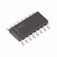
MAX791CSE+ Maxim Integrated Products, MAX791CSE+ Datasheet - Page 12

MAX791CSE+
Manufacturer Part Number
MAX791CSE+
Description
IC MPU SUPERVISOR CIRCUIT 16SOIC
Manufacturer
Maxim Integrated Products
Type
Battery Backup Circuitr
Datasheet
1.MAX791CSE.pdf
(19 pages)
Specifications of MAX791CSE+
Number Of Voltages Monitored
1
Output
Push-Pull, Totem Pole
Reset
Active Low
Reset Timeout
140 ms Minimum
Voltage - Threshold
4.65V
Operating Temperature
0°C ~ 70°C
Mounting Type
Surface Mount
Package / Case
16-SOIC (3.9mm Width)
Monitored Voltage
4.65 V
Undervoltage Threshold
4.5 V
Overvoltage Threshold
4.75 V
Manual Reset
Resettable
Watchdog
Yes
Battery Backup Switching
Yes
Power-up Reset Delay (typ)
280 ms
Supply Voltage (max)
5.5 V
Supply Voltage (min)
0 V
Supply Current (typ)
150 uA
Maximum Power Dissipation
696 mW
Mounting Style
SMD/SMT
Maximum Operating Temperature
+ 70 C
Chip Enable Signals
Yes
Minimum Operating Temperature
0 C
Output Type
Active Low or Open Drain or Push-Pull
Power Fail Detection
Yes
Lead Free Status / RoHS Status
Lead free / RoHS Compliant
PFI is the input to the power-fail comparator. PFI has a
guaranteed input leakage of ±25nA max over tempera-
ture. The typical comparator delay is 15µs from V
V
being restored). If unused, connect this input to
ground.
The Power-Fail Output (PFO) goes low when PFI goes
below 1.25V. It typically sinks 3.2mA with a saturation
voltage of 0.1V. With PFI above 1.25V, PFO is actively
pulled to V
divider to an unregulated supply allows PFO to gener-
ate an NMI as the unregulated power begins to fall
(Figure 9b). If the unregulated supply is inaccessible,
Microprocessor Supervisory Circuit
Figure 9. a) If the unregulated supply is inaccessible,
LOWLINE generates the NMI for the µP. b) Use PFO to gener-
ate the µP NMI if the unregulated supply is inaccessible.
12
OL
REGULATED
a)
b)
SUPPLY
FROM
(power failing), and 55µs from V
______________________________________________________________________________________
REGULATOR
0.1µF
VOLTAGE
OUT
3
V
CC
. Connecting PFI through a voltage-
0.1
µF
7
3
MAX791
4
GND
PFI
V
LOWLINE
CC
VBATT
RESET
MAX791
V
4
WDI
GND
OUT
VBATT
RESET
2
1
15
10
11
V
PFO
WDI
OUT
2
1
15
6
11
3.0V
0.1µF
Power-Fail Output
3.0V
0.1µF
IH
Power-Fail Input
RESET
NMI
I/O LINE
POWER TO
CMOS RAM
µP POWER
to V
µP
RESET
NMI
I/O LINE
POWER TO
CMOS RAM
OH
µP POWER
µP
(power
IL
to
use LOWLINE to generate the NMI. The LOWLINE
threshold is typically 150mV above the reset threshold
(see LOWLINE Output section).
The MAX791 requires two conditions to switch to bat-
tery-backup mode: 1) V
threshold; 2) V
the status of the inputs and outputs in battery-backup
mode.
Table 1. Input and Output States in
Battery-Backup Mode
* V
backup mode.
PIN
10
11
12
13
14
15
16
CC
1
2
3
4
5
6
7
8
9
must be below the reset threshold to enter battery-
–
—
L
BATT ON
–
C
O
—
VBATT
–
R
–
W
NAME
—
—
–
C
V
–
W
GND
E
—
—
–
P
SWT
–
V
WDI
—
W
E
—
PFI
–
M
—
D
OUT
E
—
–
—
F
—
CC
—
D
S
OUT
—
—
L
R
—
P
O
–
—
IN
—
E
–
O
—
CC
I
–
O
N
T
–
–
—
E
–
must be below VBATT. Table 1 lists
Supply current is 1µA maximum.
V
an internal PMOS switch.
Battery-switchover comparator
monitors V
GND—0V reference for all signals.
Logic high. The open-circuit output is
equal to V
The power-fail comparator remains
active in the battery-backup mode for
V
voltage,
The power-fail comparator remains
active in the battery-backup mode for
V
SWT is ignored.
– –
M
Logic low*
WDI is ignored, and goes high
impedance.
Logic high. The open-circuit output
voltage is equal to V
High impedance
Logic high. The open-circuit output
voltage is equal to V
Logic low*
Logic high. The open-circuit output
voltage is equal to V
—
OUT
CC
CC
R
–
is ignored.
≥ VBATT - 1.2V typ. Below this
≥ VBATT - 1.2V typ.
CC
is connected to VBATT through
Battery-Backup Mode
–
P
—
must be below the reset
F
OUT
—
CC
O
–
is forced low.
for active switchover.
.
STATUS
OUT
OUT
OUT
.
.
.


