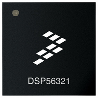
DSP56321VF200 Freescale Semiconductor, DSP56321VF200 Datasheet - Page 32

DSP56321VF200
Manufacturer Part Number
DSP56321VF200
Description
IC DSP 24BIT 200MHZ 196-BGA
Manufacturer
Freescale Semiconductor
Series
DSP563xxr
Type
Fixed Pointr
Datasheet
1.DSP56321VL200R2.pdf
(84 pages)
Specifications of DSP56321VF200
Interface
Host Interface, SSI, SCI
Clock Rate
200MHz
Non-volatile Memory
ROM (576 B)
On-chip Ram
576kB
Voltage - I/o
3.30V
Voltage - Core
1.60V
Operating Temperature
-40°C ~ 100°C
Mounting Type
*
Package / Case
196-MAPBGA
Lead Free Status / RoHS Status
Contains lead / RoHS non-compliant
Available stocks
Company
Part Number
Manufacturer
Quantity
Price
Company:
Part Number:
DSP56321VF200
Manufacturer:
MOT
Quantity:
1 831
Company:
Part Number:
DSP56321VF200
Manufacturer:
Freescale Semiconductor
Quantity:
10 000
Company:
Part Number:
DSP56321VF200R2
Manufacturer:
Freescale Semiconductor
Quantity:
10 000
Specifications
2-12
Notes:
No.
115 Address valid to RD
116 RD assertion pulse width
117 RD deassertion to
118 TA setup before RD or
119 TA hold after RD or WR
assertion
address not valid
WR deassertion
deassertion
1.
2.
3.
4.
5.
Characteristics
WS is the number of wait states specified in the BCR. The value is given for the minimum for a given category. (For example,
for a category of [3 ≤ WS ≤ 7] timing is specified for 3 wait states.) Three wait states is the minimum value otherwise.
Timings 100 and 107 are guaranteed by design, not tested.
All timings are measured from 0.5 × V
The WS number applies to the access in which the deassertion of WR occurs and assumes the next access uses a minimal
number of wait states.
Timing 118 is relative to the deassertion edge of RD or WR even if TA remains asserted.
Note: Address lines A[0–17] hold their state after a
read or write operation. AA[0–3] do not hold their
state after a read or write operation.
A[0–17]
D[0–23]
5
AA[0–3]
WR
RD
TA
Symbol
—
—
—
—
—
Table 2-8.
(WS + 0.25) × T
Figure 2-10.
0.25 × T
1.25 × T
2.25 × T
DSP56321 Technical Data, Rev. 11
Expression
0.5 × T
[3 ≤ WS ≤ 7]
[WS ≥ 3]
[WS ≥ 8]
CCQH
113
C
C
C
C
to 0.5 × V
− 2.0
+ 2.0
− 4.0
− 4.0
SRAM Timing (Continued)
C
1
− 3.0
SRAM Read Access
CCQH
104
13.25
Min
2.25
7.25
3.25
0.5
200 MHz
0
.
100
Max
—
—
—
—
—
—
105
116
11.59
Min
1.69
6.24
3.14
0.3
220 MHz
0
118
Max
—
—
—
—
—
—
Data
In
10.55
Min
1.21
5.38
3.04
0.1
240 MHz
0
Max
Freescale Semiconductor
117
106
—
—
—
—
—
—
119
–0.18
Min
8.81
0.54
4.18
2.91
275 MHz
0
Max
—
—
—
—
—
—
Unit
ns
ns
ns
ns
ns
ns


