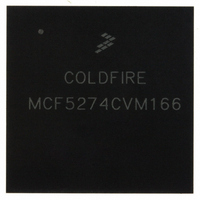
MCF5274CVM166 Freescale Semiconductor, MCF5274CVM166 Datasheet - Page 32

MCF5274CVM166
Manufacturer Part Number
MCF5274CVM166
Description
IC MPU 32BIT 166MHZ 256-MAPBGA
Manufacturer
Freescale Semiconductor
Series
MCF527xr
Datasheet
1.MCF5274LVM166J.pdf
(44 pages)
Specifications of MCF5274CVM166
Core Processor
Coldfire V2
Core Size
32-Bit
Speed
166MHz
Connectivity
EBI/EMI, Ethernet, I²C, SPI, UART/USART, USB
Peripherals
DMA, WDT
Number Of I /o
69
Program Memory Type
ROMless
Ram Size
64K x 8
Voltage - Supply (vcc/vdd)
1.4 V ~ 1.6 V
Oscillator Type
External
Operating Temperature
-40°C ~ 85°C
Package / Case
256-MAPBGA
Embedded Interface Type
I2C, SPI, USB, UART
Digital Ic Case Style
BGA
No. Of Pins
256
Operating Temperature Range
-40°C To +85°C
Processor Type
68K/ColdFire V2
Rohs Compliant
Yes
Family Name
MCF5xxx
Device Core
ColdFire
Device Core Size
32b
Frequency (max)
166MHz
Instruction Set Architecture
RISC
Operating Supply Voltage (max)
1.6V
Operating Supply Voltage (min)
1.4V
Operating Temp Range
-40C to 85C
Operating Temperature Classification
Industrial
Mounting
Surface Mount
Pin Count
256
Package Type
MA-BGA
Lead Free Status / RoHS Status
Lead free / RoHS Compliant
Eeprom Size
-
Program Memory Size
-
Data Converters
-
Lead Free Status / Rohs Status
Compliant
Available stocks
Company
Part Number
Manufacturer
Quantity
Price
Company:
Part Number:
MCF5274CVM166
Manufacturer:
Freescale Semiconductor
Quantity:
10 000
Electrical Characteristics
8.9
GPIO can be configured for certain pins of the QSPI, DDR control, timers, UARTS, FEC0, FEC1,
Interrupts and USB interfaces. When in GPIO mode the timing specification for these pins is given in
Table 16
32
NUM
G1
G2
G3
G4
SD_SRAS,SD_SCAS
SD_CSn,SD_WE,
and
General Purpose I/O Timing
CLKOUT High to GPIO Output Valid
CLKOUT High to GPIO Output Invalid
GPIO Input Valid to CLKOUT High
CLKOUT High to GPIO Input Invalid
SD_DQS[3:2]
SD_DQS[3:2]
Figure
CLKOUT
CLKOUT
D[31:16]
D[31:16]
A[13:0]
MCF5275 Integrated Microprocessor Family Hardware Specification, Rev. 4
15.
DD4
Characteristic
ROW
CMD
Figure 14. DDR Read Timing
DD1
Table 16. GPIO Timing
DD5
COL
CL=2
CL=2.5
DQS Read
DD2
Preamble
DD10
Symbol
t
t
CHPOV
t
CHPOI
t
PVCH
DQS Read
CHPI
Preamble
DD3
WD1 WD2 WD3 WD4
Min
WD1 WD2 WD3 WD4
1.0
1.5
—
9
DD9
Freescale Semiconductor
DQS Read
Postamble
Max
10
—
—
—
DQS Read
Postamble
Unit
ns
ns
ns
ns


