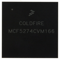
MCF5274CVM166 Freescale Semiconductor, MCF5274CVM166 Datasheet - Page 9

MCF5274CVM166
Manufacturer Part Number
MCF5274CVM166
Description
IC MPU 32BIT 166MHZ 256-MAPBGA
Manufacturer
Freescale Semiconductor
Series
MCF527xr
Datasheet
1.MCF5274LVM166J.pdf
(44 pages)
Specifications of MCF5274CVM166
Core Processor
Coldfire V2
Core Size
32-Bit
Speed
166MHz
Connectivity
EBI/EMI, Ethernet, I²C, SPI, UART/USART, USB
Peripherals
DMA, WDT
Number Of I /o
69
Program Memory Type
ROMless
Ram Size
64K x 8
Voltage - Supply (vcc/vdd)
1.4 V ~ 1.6 V
Oscillator Type
External
Operating Temperature
-40°C ~ 85°C
Package / Case
256-MAPBGA
Embedded Interface Type
I2C, SPI, USB, UART
Digital Ic Case Style
BGA
No. Of Pins
256
Operating Temperature Range
-40°C To +85°C
Processor Type
68K/ColdFire V2
Rohs Compliant
Yes
Family Name
MCF5xxx
Device Core
ColdFire
Device Core Size
32b
Frequency (max)
166MHz
Instruction Set Architecture
RISC
Operating Supply Voltage (max)
1.6V
Operating Supply Voltage (min)
1.4V
Operating Temp Range
-40C to 85C
Operating Temperature Classification
Industrial
Mounting
Surface Mount
Pin Count
256
Package Type
MA-BGA
Lead Free Status / RoHS Status
Lead free / RoHS Compliant
Eeprom Size
-
Program Memory Size
-
Data Converters
-
Lead Free Status / Rohs Status
Compliant
Available stocks
Company
Part Number
Manufacturer
Quantity
Price
Company:
Part Number:
MCF5274CVM166
Manufacturer:
Freescale Semiconductor
Quantity:
10 000
5
5.1
5.2
Freescale Semiconductor
•
•
•
•
Use a 4-layer printed circuit board with the VDD and GND pins connected directly to the power
and ground planes for the MCF5275.
See application note AN1259 System Design and Layout Techniques for Noise Reduction in
MCU-Based Systems.
Match the PC layout trace width and routing to match trace length to operating frequency and board
impedance. Add termination (series or therein) to the traces to dampen reflections. Increase the
PCB impedance (if possible) keeping the trace lengths balanced and short. Then do cross-talk
analysis to separate traces with significant parallelism or are otherwise "noisy". Use 6 mils trace
and separation. Clocks get extra separation and more precise balancing.
33uF, 0.1 μF, and 0.01 μF across each power supply
1
2
Design Recommendations
Layout
Power Supply
Refers to pin’s primary function. All pins which are configurable for GPIO have a pullup enabled in GPIO
mode with the exception of PBUSCTL[7], PBUSCTL[4:0], PADDR, PBS, PSDRAM.
If JTAG_EN is asserted, these pins default to Alternate 1 (JTAG) functionality. The GPIO module is not
responsible for assigning these pins.
Signal Name
SD_VDD
VSSPLL
OVDD
VDD
Table 2. MCF5274 and MCF5275 Signal Information and Muxing (continued)
VSS
MCF5275 Integrated Microprocessor Family Hardware Specification, Rev. 4
GPIO
—
—
—
—
—
Alternate1
—
—
—
—
—
Alternate2 Dir.
—
—
—
—
—
I
I
I
I
I
1
E6:8, F5, F7, F8,
D8, H13, K4, N8 D6, G5, G12, L7
G5, G6, H5, H6,
E9:11, F9, F10,
F12, G11, G12,
L7, L8, M6, M7,
J6, K5, K6, L5,
256 MAPBGA
J11, J12, K11,
A1, A10, A16,
H11, H12, J5,
K12, L9, L10,
J7:10, K7:10,
E5, E12, F6,
L6, L11, M5,
N16, R7, T1,
F11, G7:10,
L12, M9:11
H7:10, J1,
MCF5274
MCF5275
K16
T16
M8
Design Recommendations
G10, H5, J5, J6,
E8:10, F9, F10,
196 MAPBGA
F7, F8, G6:9,
H10, J9, J10,
E5:7, F5, F6,
H6:9, J7, J8
MCF5274L
MCF5275L
K8:10
K5:7
L13
9


