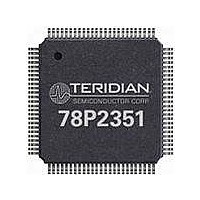
78P2351-IGT/F Maxim Integrated Products, 78P2351-IGT/F Datasheet - Page 32

78P2351-IGT/F
Manufacturer Part Number
78P2351-IGT/F
Description
LINE INTERFACE UNIT 100-LQFP
Manufacturer
Maxim Integrated Products
Specifications of 78P2351-IGT/F
Number Of Channels Per Chip
1
Propagation Delay Time
10 ns
Supply Voltage (max)
3.45 V
Supply Voltage (min)
3.15 V
Maximum Operating Temperature
+ 85 C
Package / Case
LQFP-100
Minimum Operating Temperature
- 40 C
Mounting Style
SMD/SMT
Lead Free Status / RoHS Status
Lead free / RoHS Compliant
Available stocks
Company
Part Number
Manufacturer
Quantity
Price
Company:
Part Number:
78P2351-IGT/F
Manufacturer:
VISHAY
Quantity:
14 105
Company:
Part Number:
78P2351-IGT/F
Manufacturer:
MAXIM
Quantity:
4
Company:
Part Number:
78P2351-IGT/F
Manufacturer:
Maxim Integrated
Quantity:
10 000
Note 1 – The maximum “steady state” amplitude should not exceed the 0.55V limit. Overshoots and other transients are permitted to fall into
the shaded area bounded by the amplitude levels 0.55V and 0.6V, provided that they do not exceed the steady state level by more than
0.05V.
Note 2 – For all measurements using these masks, the signal should be AC coupled, using a capacitor of not less than 0.01 µF, to the input of
the oscilloscope used for measurements. The nominal zero level for both masks should be aligned with the oscilloscope trace with no input
signal. With the signal then applied, the vertical position of the trace can be adjusted with the objective of meeting the limits of the masks. Any
such adjustment should be the same for both masks and should not exceed ±0.05V. This may be checked by removing the input signal again
and verifying that the trace lies with ±0.05V of the nominal zero level of the masks.
Note 3 – Each pulse in a coded pulse sequence should meet the limits of the relevant mask, irrespective of the state of the preceding or
succeeding pulses, with both pulse masks fixed in the same relation to a common timing reference, i.e. with their nominal start and finish
edges coincident. The masks allow for HF jitter caused by intersymbol interference in the output stage, but not for jitter present in the timing
signal associated with the source of the interface signal. When using an oscilloscope technique to determine pulse compliance with the mask,
it is important that successive traces of the pulses overlay in order to suppress the effects of low frequency jitter. This can be accomplished by
several techniques [e.g. a) triggering the oscilloscope on the measured waveform or b) providing both the oscilloscope and the pulse output
circuits with the same clock signal].
Note 4 – For the purpose of these masks, the rise time and decay time should be measured between –0.4V and 0.4V, and should not exceed
2ns.
Page: 32 of 42
ELECTRICAL SPECIFICATIONS
-0.05
-0.40
-0.45
-0.50
-0.55
-0.60
0.60
0.55
0.50
0.45
0.40
0.05
V
Figure 14 – Mask of a Pulse corresponding to a binary Zero in STM-1/STS-3 mode.
Zero Level
Nominal
(Note 2)
(Note 1)
0.1ns
1ns
1ns
0.1ns
1.608ns
2006 Teridian Semiconductor Corporation
(continued)
(Note 1)
1.608ns
0.35ns
1ns
T = 6.43ns
1.608ns
0.35ns
1ns
(Note 1)
1.608ns
0.1ns
OC-3/ STM1-E/ E4 LIU
1ns
Single Channel
Nominal
(Note 1)
1ns
0.1ns
Pulse
78P2351
Rev. 2.4


