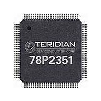
78P2351-IGT/F Maxim Integrated Products, 78P2351-IGT/F Datasheet - Page 4

78P2351-IGT/F
Manufacturer Part Number
78P2351-IGT/F
Description
LINE INTERFACE UNIT 100-LQFP
Manufacturer
Maxim Integrated Products
Specifications of 78P2351-IGT/F
Number Of Channels Per Chip
1
Propagation Delay Time
10 ns
Supply Voltage (max)
3.45 V
Supply Voltage (min)
3.15 V
Maximum Operating Temperature
+ 85 C
Package / Case
LQFP-100
Minimum Operating Temperature
- 40 C
Mounting Style
SMD/SMT
Lead Free Status / RoHS Status
Lead free / RoHS Compliant
Available stocks
Company
Part Number
Manufacturer
Quantity
Price
Company:
Part Number:
78P2351-IGT/F
Manufacturer:
VISHAY
Quantity:
14 105
Company:
Part Number:
78P2351-IGT/F
Manufacturer:
MAXIM
Quantity:
4
Company:
Part Number:
78P2351-IGT/F
Manufacturer:
Maxim Integrated
Quantity:
10 000
FUNCTIONAL DESCRIPTION
The 78P2351 contains all the necessary transmit
and
139.264Mbps and 155.52Mbps line interfaces and
the digital universe. The chip is controllable through
pins or serial port register settings.
MODE SELECTION
The SDO_E4 pin or E4 register bit determines which
rate the device operates in according to the table
below.
selects the reference clock frequency.
The SEN_CMI pin or CMI register bit enables the
CMI encoder/decoder and selects one of two media
for reception and transmission: 75Ω coaxial cable in
CMI coding or optical fiber in Fiber (NRZ) mode.
The SDI_PAR pin or PAR register bit selects the
interface to the framer to be 4-bit parallel CMOS or
serial LVPECL.
different transmit timing modes available. See
TRANSMITTER OPERATION section for more info.
REFERENCE CLOCK
The 78P2351 requires a reference clock supplied to
the CKREFP/N pins. This reference clock is used
for clock recovery in the Rx DLL and Tx DLL. It is
also used for transmit re-timing in the synchronous
transmit modes.
OPERATION section for timing requirements during
synchronous (re-timing) transmit modes.
For reference frequencies of 77.76MHz or lower, the
device accepts a single ended CMOS clock at
CKREFP (with CKREFN grounded). For reference
frequencies of 139.264 or 155.52MHz, the device
accepts a differential LVPECL clock input at
CKREFP/N.
Page: 4 of 42
Rate
E4
STM-1, STS-3, OC-3
Media (coding)
75Ω Coax (CMI)
Fiber (NRZ)
In hardware mode (pin control) the SPSL pin
must be low.
In software mode (SPSL pin high), control pins
are disabled and the 78P2351 must be
configured via the 4-wire serial port.
receive circuitry
This control combined with CKSL also
For each interface there are
Refer to the TRANSMITTER
SDO_E4 pin
High
Low
SEN_CMI pin
High
Low
for connection
2006 Teridian Semiconductor Corporation
E4 bit
1
0
CMI bit
1
0
between
The frequency of this reference input is controlled by
the rate selection and the CKSL control pin or
register bit.
RECEIVER OPERATION
The receiver accepts serial data, at 155.52Mbps or
139.264Mbps from the RXP/N inputs. In CMI mode,
the input is differentially terminated with 75Ω and
transformer-coupled to a coaxial connector. In Fiber
(NRZ) mode, the input is differentially terminated
with 100Ω and AC-coupled to an optical transceiver
module. For board designs utilizing both coax and
fiber media options, an analog switch or mechanical
relay is required to switch between the different
terminations and media paths.
The recovered CMI signal first enters an AGC and
anadaptive equalizer designed to overcome inter-
symbol interference caused by long cable lengths.
The variable gain differential amplifier automatically
controls the gain to maintain a constant voltage level
output regardless of the input voltage level. Note
that in Fiber (NRZ) mode, the input signals bypass
the adaptive equalizer.
The outputs of the data comparators are connected
to the clock recovery circuits. The clock recovery
system employs a Delay Locked Loop (DLL), which
uses a reference frequency derived from the clock
applied to the CKREFP/N pins.
In serial mode, the clock and data are decoded and
transmitted through the LVPECL drivers. In parallel
mode, the data is decoded and converted into four
bit parallel segments before being transmitted
through the CMOS drivers. Note that in Fiber (NRZ)
mode, the CMI decoder is bypassed.
Receiver Monitor Mode
In CMI mode, the SCK_MON pin or MON register bit
enables the receiver’s monitor mode which adds
approximately 20dB of flat gain to the receive signal
before equalization. Rx Monitor Mode can handle
20dB of flat loss typical of monitoring points with up
to 6dB of cable loss.
detection is disabled during Rx Monitor Mode.
CKSL pin
Low
Float
High
0 0
1 0
1 1
CKSL[1:0] bits
SDO_E4 low
155.52MHz
155.52MHz
19.44MHz
77.76MHz
19.44MHz
77.76MHz
E4 bit = 0
OC-3/ STM1-E/ E4 LIU
Reference Frequency
Note that Loss of Signal
Single Channel
SDO_E4 high
139.264MHz
139.264MHz
17.408MHz
17.408MHz
E4 bit = 1
78P2351
N/A
N/A
Rev. 2.4


