MW6IC2015NBR1 Freescale Semiconductor, MW6IC2015NBR1 Datasheet - Page 2
MW6IC2015NBR1
Manufacturer Part Number
MW6IC2015NBR1
Description
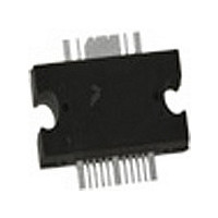
IC PWR AMP RF 26V 15W TO-272-16
Manufacturer
Freescale Semiconductor
Type
Power Amplifierr
Datasheet
1.MW6IC2015GNBR1.pdf
(28 pages)
Specifications of MW6IC2015NBR1
Current - Supply
100mA
Frequency
1.8GHz ~ 1.99GHz
Gain
26dB
Package / Case
TO-272-16
Rf Type
Cellular, W-CDMA, GSM, EDGE, TDMA, CDMA
Voltage - Supply
26V
Number Of Channels
1
Frequency (max)
1.99GHz
Power Supply Requirement
Single
Single Supply Voltage (min)
26V
Single Supply Voltage (typ)
28V
Single Supply Voltage (max)
32V
Dual Supply Voltage (min)
Not RequiredV
Dual Supply Voltage (typ)
Not RequiredV
Dual Supply Voltage (max)
Not RequiredV
Pin Count
16
Mounting
Surface Mount
Lead Free Status / RoHS Status
Lead free / RoHS Compliant
Noise Figure
-
P1db
-
Test Frequency
-
Lead Free Status / Rohs Status
Compliant
Available stocks
Company
Part Number
Manufacturer
Quantity
Price

Part Number:
MW6IC2015NBR1
Manufacturer:
FREESCALE
Quantity:
20 000


MW6IC2015NBR1 MW6IC2015GNBR1
2
Table 1. Maximum Ratings
Table 2. Thermal Characteristics
Table 3. ESD Protection Characteristics
Table 4. Moisture Sensitivity Level
Table 5. Electrical Characteristics
Functional Tests (In Freescale 1930 - 1990 MHz Test Fixture, 50 ohm system) V
PEP, f1 = 1930 MHz, f2 = 1930.1 MHz, Two - Tone CW
Typical Two - Tone Performances (In Freescale Test Fixture, 50 ohm system) V
15 W PEP, 1805 - 1880 MHz, Two - Tone CW, 100 kHz Tone Spacing
Drain - Source Voltage
Gate - Source Voltage
Storage Temperature Range
Case Operating Temperature
Operating Junction Temperature
Input Power
Thermal Resistance, Junction to Case
Human Body Model (per JESD22 - A114)
Machine Model (per EIA/JESD22 - A115)
Charge Device Model (per JESD22 - C101)
Per JESD 22 - A113, IPC/JEDEC J - STD - 020
Power Gain
Power Added Efficiency
Intermodulation Distortion
Input Return Loss
Power Gain
Power Added Efficiency
Intermodulation Distortion
Input Return Loss
1. Continuous use at maximum temperature will affect MTTF.
2. MTTF calculator available at http://www.freescale.com/rf. Select Software & Tools/Development Tools/Calculators to access
3. Refer to AN1955, Thermal Measurement Methodology of RF Power Amplifiers. Go to http://www.freescale.com/rf.
Final Application
(P
Driver Application
(P
MTTF calculators by product.
Select Documentation/Application Notes - AN1955.
out
out
= 15 W CW)
= 3 W CW)
Test Methodology
Characteristic
Test Methodology
Characteristic
(1,2)
Rating
(T
C
Stage 1, 26 Vdc, I
Stage 2, 26 Vdc, I
Stage 1, 26 Vdc, I
Stage 2, 26 Vdc, I
= 25°C unless otherwise noted)
DQ1
DQ2
DQ1
DQ2
= 100 mA
= 170 mA
= 130 mA
= 170 mA
Rating
3
Symbol
PAE
PAE
IMD
IMD
G
G
IRL
IRL
DD
DD
ps
ps
= 26 Vdc, I
= 26 Vdc, I
Symbol
Symbol
V
R
V
T
T
P
Package Peak Temperature
T
DSS
θJC
stg
GS
C
in
J
Min
24
26
—
—
—
—
—
—
DQ1
DQ1
= 100 mA, I
= 100 mA, I
260
1A (Minimum)
III (Minimum)
A (Minimum)
Typ
- 30
- 30
- 10
26
28
26
28
—
- 65 to +150
Value
Class
- 0.5, +68
- 0.5, +6
DQ2
Value
DQ2
150
225
4.3
1.2
4.3
1.3
Freescale Semiconductor
20
= 170 mA, P
(2,3)
= 170 mA, P
Max
- 27
- 10
—
—
—
—
—
—
RF Device Data
out
out
(continued)
=
= 15 W
°C/W
Unit
dBm
Unit
Unit
Vdc
Vdc
Unit
°C
dBc
dBc
°C
°C
°C
dB
dB
dB
dB
%
%
Related parts for MW6IC2015NBR1
Image
Part Number
Description
Manufacturer
Datasheet
Request
R

Part Number:
Description:
Manufacturer:
Freescale Semiconductor, Inc
Datasheet:
Part Number:
Description:
Manufacturer:
Freescale Semiconductor, Inc
Datasheet:
Part Number:
Description:
Manufacturer:
Freescale Semiconductor, Inc
Datasheet:
Part Number:
Description:
Manufacturer:
Freescale Semiconductor, Inc
Datasheet:
Part Number:
Description:
Manufacturer:
Freescale Semiconductor, Inc
Datasheet:
Part Number:
Description:
Manufacturer:
Freescale Semiconductor, Inc
Datasheet:
Part Number:
Description:
Manufacturer:
Freescale Semiconductor, Inc
Datasheet:
Part Number:
Description:
Manufacturer:
Freescale Semiconductor, Inc
Datasheet:
Part Number:
Description:
Manufacturer:
Freescale Semiconductor, Inc
Datasheet:
Part Number:
Description:
Manufacturer:
Freescale Semiconductor, Inc
Datasheet:
Part Number:
Description:
Manufacturer:
Freescale Semiconductor, Inc
Datasheet:
Part Number:
Description:
Manufacturer:
Freescale Semiconductor, Inc
Datasheet:
Part Number:
Description:
Manufacturer:
Freescale Semiconductor, Inc
Datasheet:
Part Number:
Description:
Manufacturer:
Freescale Semiconductor, Inc
Datasheet:
Part Number:
Description:
Manufacturer:
Freescale Semiconductor, Inc
Datasheet: