MW6IC2015NBR1 Freescale Semiconductor, MW6IC2015NBR1 Datasheet - Page 27
MW6IC2015NBR1
Manufacturer Part Number
MW6IC2015NBR1
Description
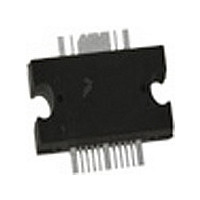
IC PWR AMP RF 26V 15W TO-272-16
Manufacturer
Freescale Semiconductor
Type
Power Amplifierr
Datasheet
1.MW6IC2015GNBR1.pdf
(28 pages)
Specifications of MW6IC2015NBR1
Current - Supply
100mA
Frequency
1.8GHz ~ 1.99GHz
Gain
26dB
Package / Case
TO-272-16
Rf Type
Cellular, W-CDMA, GSM, EDGE, TDMA, CDMA
Voltage - Supply
26V
Number Of Channels
1
Frequency (max)
1.99GHz
Power Supply Requirement
Single
Single Supply Voltage (min)
26V
Single Supply Voltage (typ)
28V
Single Supply Voltage (max)
32V
Dual Supply Voltage (min)
Not RequiredV
Dual Supply Voltage (typ)
Not RequiredV
Dual Supply Voltage (max)
Not RequiredV
Pin Count
16
Mounting
Surface Mount
Lead Free Status / RoHS Status
Lead free / RoHS Compliant
Noise Figure
-
P1db
-
Test Frequency
-
Lead Free Status / Rohs Status
Compliant
Available stocks
Company
Part Number
Manufacturer
Quantity
Price

Part Number:
MW6IC2015NBR1
Manufacturer:
FREESCALE
Quantity:
20 000


RF Device Data
Freescale Semiconductor
Application Notes
• AN1907: Solder Reflow Attach Method for High Power RF Devices in Plastic Packages
• AN1955: Thermal Measurement Methodology of RF Power Amplifiers
• AN1977: Quiescent Current Thermal Tracking Circuit in the RF Integrated Circuit Family
• AN1987: Quiescent Current Control for the RF Integrated Circuit Device Family
• AN3263: Bolt Down Mounting Method for High Power RF Transistors and RFICs in Over - Molded Plastic Packages
Engineering Bulletins
• EB212: Using Data Sheet Impedances for RF LDMOS Devices
Revision
Refer to the following documents to aid your design process.
The following table summarizes revisions to this document.
2
3
Dec. 2008
Feb. 2007
Date
• Added “and TD - SCDMA” to data sheet description paragraph, p. 1.
• Updated verbiage on Typical Performances table, p. 2
• Corrected V
• Updated Part Numbers in Tables 6 and 7, Component Designations and Values, to RoHS compliant part
• Adjusted scale for Figs. 7 and 25, Two - Tone Power Gain versus Output Power, Figs. 8 and 26,
• Replaced Figure 18, MTTF versus Junction Temperature with updated graph. Removed Amps
• Corrected Series Impedance data table test conditions, Figs. 20 and 36, p. 10, 16
• Added TD - SCDMA test circuit schematic, component designations and values, component layout, typical
• Added Product Documentation and Revision History, p. 27
• Modified data sheet to reflect RF Test Reduction described in Product and Process Change Notification
• Changed 220°C to 225°C in Capable Plastic Package bullet, p. 1
• Added Footnote 1 to Quiescent Current Temperature bullet under Features section and to callout in Fig. 1,
• Changed Storage Temperature Range in Max Ratings table from - 65 to +200 to - 65 to +150 for
• Added Case Operating Temperature limit to the Maximum Ratings table and set limit to 150°C, p. 2
• Operating Junction Temperature increased from 200°C to 225°C in Maximum Ratings table and related
• Updated Part Numbers in Tables 6, 7, and 8 Component Designations and Values, to latest RoHS compliant
• Removed lower voltage tests from Figs. 13 and 31, Power Gain versus Output Power, due to fixed tuned
• Adjust scale for Fig. 27, Intermodulation Distortion Products versus Tone Spacing, to show wider dynamic
• Replaced Case Outline 1329A - 03 with 1329A - 04, Issue F, p. 1, 24 - 26. Added pin numbers 1 through 17.
• Replaced Case Outline 1329 - 09, Issue L, with 1329 - 09, Issue M, p. 21 - 23. Added pin numbers 1 through
Circuit Component Layout, p. 5, 12
numbers, p. 4, 11
Intermodulation Distortion Products versus Output Power, Figs. 11 and 29, 2 - Carrier W - CDMA ACPR, IM3,
Power Gain and Power Added Efficiency versus Output Power, Figs. 12 and 30, Power Gain and Power
Added Efficiency versus CW Output Power, Figs. 16 and 34, EVM and Power Added Efficiency versus
Output Power, Figs. 17 and 35, Spectral Regrowth at 400 and 600 kHz versus Output Power, to better
match the device’s capabilities, p. 6 - 8, 13 - 15
operating characteristics and location of MTTF calculator for device, p. 9
characteristic curves, test signal and series impedance, p. 17 - 20.
number, PCN13232, p. 1, 2
Functional Block Diagram, p. 1
standardization across products, p. 2
“Continuous use at maximum temperature will affect MTTF” footnote added, p. 2
part numbers, p. 4, 11, 17
fixture limitations, p. 7, 14
range, p. 14
Corrected mm dimension L for gull - wing foot from 4.90 - 5.06 Min - Max to 0.46 - 0.61 Min - Max. Corrected L1
mm dimension from .025 BSC to 0.25 BSC. Added JEDEC Standard Package Number.
17.
BIAS
and V
PRODUCT DOCUMENTATION
SUPPLY
REVISION HISTORY
callouts, Figs. 3 and 21, Test Circuit Schematic, p. 4, 11, Figs. 4 and 22, Test
Description
MW6IC2015NBR1 MW6IC2015GNBR1
2
and listed
27
Related parts for MW6IC2015NBR1
Image
Part Number
Description
Manufacturer
Datasheet
Request
R

Part Number:
Description:
Manufacturer:
Freescale Semiconductor, Inc
Datasheet:
Part Number:
Description:
Manufacturer:
Freescale Semiconductor, Inc
Datasheet:
Part Number:
Description:
Manufacturer:
Freescale Semiconductor, Inc
Datasheet:
Part Number:
Description:
Manufacturer:
Freescale Semiconductor, Inc
Datasheet:
Part Number:
Description:
Manufacturer:
Freescale Semiconductor, Inc
Datasheet:
Part Number:
Description:
Manufacturer:
Freescale Semiconductor, Inc
Datasheet:
Part Number:
Description:
Manufacturer:
Freescale Semiconductor, Inc
Datasheet:
Part Number:
Description:
Manufacturer:
Freescale Semiconductor, Inc
Datasheet:
Part Number:
Description:
Manufacturer:
Freescale Semiconductor, Inc
Datasheet:
Part Number:
Description:
Manufacturer:
Freescale Semiconductor, Inc
Datasheet:
Part Number:
Description:
Manufacturer:
Freescale Semiconductor, Inc
Datasheet:
Part Number:
Description:
Manufacturer:
Freescale Semiconductor, Inc
Datasheet:
Part Number:
Description:
Manufacturer:
Freescale Semiconductor, Inc
Datasheet:
Part Number:
Description:
Manufacturer:
Freescale Semiconductor, Inc
Datasheet:
Part Number:
Description:
Manufacturer:
Freescale Semiconductor, Inc
Datasheet: