MW6IC2015NBR1 Freescale Semiconductor, MW6IC2015NBR1 Datasheet - Page 3
MW6IC2015NBR1
Manufacturer Part Number
MW6IC2015NBR1
Description
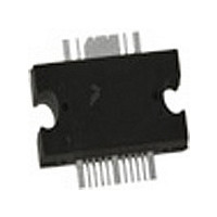
IC PWR AMP RF 26V 15W TO-272-16
Manufacturer
Freescale Semiconductor
Type
Power Amplifierr
Datasheet
1.MW6IC2015GNBR1.pdf
(28 pages)
Specifications of MW6IC2015NBR1
Current - Supply
100mA
Frequency
1.8GHz ~ 1.99GHz
Gain
26dB
Package / Case
TO-272-16
Rf Type
Cellular, W-CDMA, GSM, EDGE, TDMA, CDMA
Voltage - Supply
26V
Number Of Channels
1
Frequency (max)
1.99GHz
Power Supply Requirement
Single
Single Supply Voltage (min)
26V
Single Supply Voltage (typ)
28V
Single Supply Voltage (max)
32V
Dual Supply Voltage (min)
Not RequiredV
Dual Supply Voltage (typ)
Not RequiredV
Dual Supply Voltage (max)
Not RequiredV
Pin Count
16
Mounting
Surface Mount
Lead Free Status / RoHS Status
Lead free / RoHS Compliant
Noise Figure
-
P1db
-
Test Frequency
-
Lead Free Status / Rohs Status
Compliant
Available stocks
Company
Part Number
Manufacturer
Quantity
Price

Part Number:
MW6IC2015NBR1
Manufacturer:
FREESCALE
Quantity:
20 000


RF Device Data
Freescale Semiconductor
Table 5. Electrical Characteristics
Typical Performances (In Freescale Test Fixture, 50 ohm system) V
1930 - 1990 MHz
Typical GSM EDGE Performances (In Freescale GSM EDGE Test Fixture, 50 ohm system) V
P
out
Saturated Pulsed Output Power, CW
Quiescent Current Accuracy over Temperature
Gain Flatness in 30 MHz Bandwidth @ P
Average Deviation from Linear Phase in 30 MHz Bandwidth
Average Group Delay @ P
Part - to - Part Insertion Phase Variation @ P
Power Gain
Power Added Efficiency
Error Vector Magnitude
Spectral Regrowth at 400 kHz Offset
Spectral Regrowth at 600 kHz Offset
1. Refer to AN1977, Quiescent Current Thermal Tracking Circuit in the RF Integrated Circuit Family and to AN1987, Quiescent Current Control
(8 μsec(on), 1 msec(off))
with 1.8 kΩ Gate Feed Resistors ( - 10 to 85°C)
@ P
Six Sigma Window
= 3 W Avg., 1805 - 1990 MHz and 1930 - 1990 MHz EDGE Modulation
for the RF Integrated Circuit Device Family. Go to http://www.freescale.com/rf. Select Documentation/Application Notes - AN1977 or
AN1987.
out
= 3 W CW
out
Characteristic
= 3 W CW Including Output Matching
(T
out
C
out
= 25°C unless otherwise noted) (continued)
= 3 W CW
= 3 W CW,
(1)
DD
= 26 Vdc, I
Symbol
Delay
EVM
ΔI
PAE
SR1
SR2
P
G
ΔΦ
G
Φ
sat
QT
ps
F
DQ1
= 100 mA, I
Min
—
—
—
—
—
—
—
—
—
—
—
DD
MW6IC2015NBR1 MW6IC2015GNBR1
= 26 Vdc, I
DQ2
= 170 mA, 1805 - 1880 MHz and
Typ
±15
- 69
- 78
0.3
2.7
0.8
35
±3
±1
27
19
DQ1
= 130 mA, I
Max
—
—
—
—
—
—
—
—
—
—
—
DQ2
= 170 mA,
Unit
dBc
dBc
dB
dB
W
ns
%
%
%
°
°
3
Related parts for MW6IC2015NBR1
Image
Part Number
Description
Manufacturer
Datasheet
Request
R

Part Number:
Description:
Manufacturer:
Freescale Semiconductor, Inc
Datasheet:
Part Number:
Description:
Manufacturer:
Freescale Semiconductor, Inc
Datasheet:
Part Number:
Description:
Manufacturer:
Freescale Semiconductor, Inc
Datasheet:
Part Number:
Description:
Manufacturer:
Freescale Semiconductor, Inc
Datasheet:
Part Number:
Description:
Manufacturer:
Freescale Semiconductor, Inc
Datasheet:
Part Number:
Description:
Manufacturer:
Freescale Semiconductor, Inc
Datasheet:
Part Number:
Description:
Manufacturer:
Freescale Semiconductor, Inc
Datasheet:
Part Number:
Description:
Manufacturer:
Freescale Semiconductor, Inc
Datasheet:
Part Number:
Description:
Manufacturer:
Freescale Semiconductor, Inc
Datasheet:
Part Number:
Description:
Manufacturer:
Freescale Semiconductor, Inc
Datasheet:
Part Number:
Description:
Manufacturer:
Freescale Semiconductor, Inc
Datasheet:
Part Number:
Description:
Manufacturer:
Freescale Semiconductor, Inc
Datasheet:
Part Number:
Description:
Manufacturer:
Freescale Semiconductor, Inc
Datasheet:
Part Number:
Description:
Manufacturer:
Freescale Semiconductor, Inc
Datasheet:
Part Number:
Description:
Manufacturer:
Freescale Semiconductor, Inc
Datasheet: