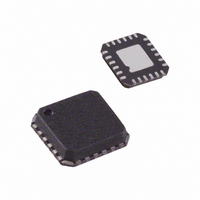
ADL5382ACPZ-R7 Analog Devices Inc, ADL5382ACPZ-R7 Datasheet - Page 21

ADL5382ACPZ-R7
Manufacturer Part Number
ADL5382ACPZ-R7
Description
IC DEMOD QUAD 700M2.7GHZ 24LFCSP
Manufacturer
Analog Devices Inc
Datasheet
1.ADL5382ACPZ-R7.pdf
(28 pages)
Specifications of ADL5382ACPZ-R7
Design Resources
Interfacing ADL5382 to AD9262 as an RF-to-Bits Solution (CN0062)
Function
Demodulator
Lo Frequency
700MHz ~ 2.7GHz
Rf Frequency
700MHz ~ 2.7GHz
P1db
14.5dBm
Gain
3.3dB
Noise Figure
17.6dB
Current - Supply
220mA
Voltage - Supply
4.75 V ~ 5.25 V
Package / Case
24-VFQFN, 24-CSP Exposed Pad
Frequency Range
700MHz To 2.7GHz
Rf Type
Quadrature
Supply Voltage Range
4.75V To 5.25V
Rf Ic Case Style
LFCSP
No. Of Pins
24
Operating Temperature Range
-40°C To +85°C
Lead Free Status / RoHS Status
Lead free / RoHS Compliant
Other names
ADL5382ACPZ-R7TR
Available stocks
Company
Part Number
Manufacturer
Quantity
Price
Company:
Part Number:
ADL5382ACPZ-R7
Manufacturer:
Analog Devices Inc
Quantity:
1 881
Part Number:
ADL5382ACPZ-R7
Manufacturer:
ADI/亚德诺
Quantity:
20 000
CHARACTERIZATION SETUPS
Figure 57 to Figure 59 show the general characterization bench
setups used extensively for the ADL5382. The setup shown in
Figure 59 was used to do the bulk of the testing and used sinusoidal
signals on both the LO and RF inputs. An automated Agilent
VEE program was used to control the equipment over the IEEE
bus. This setup was used to measure gain, IP1dB, IIP2, IIP3, I/Q
gain match, and quadrature error. The ADL5382 characterization
board had a 9-to-1 impedance transformer on each of the
differential baseband ports to do the differential-to-single-
ended conversion, which presented a 450 Ω differential load to
each baseband port, when interfaced with 50 Ω test equipment.
For all measurements of the ADL5382, the loss of the RF input
balun (the M/A-COM ETC1-1-13 was used on RF input during
characterization) was de-embedded.
SIGNAL GENERATOR
POWER SUPPLY
AGILENT 8665B
HP 6235A
GND
V
POS
Figure 57. General Noise Figure Measurement Setup
CHAR BOARD
ADL5382
RF
LO
SNS
OUTPUT
Rev. 0 | Page 21 of 28
CONTROL
Q
I
IEEE
50Ω
R1
LOW-PASS
The two setups shown in Figure 57 and Figure 58 were used for
making NF measurements. Figure 57 shows the setup for
measuring NF with no blocker signal applied while Figure 58
was used to measure NF in the presence of a blocker. For both
setups, the noise was measured at a baseband frequency of
10 MHz. For the case where a blocker was applied, the output
blocker was at a 15 MHz baseband frequency. Note that great
care must be taken when measuring NF in the presence of a
blocker. The RF blocker generator must be filtered to prevent its
noise (which increases with increasing generator output power)
from swamping the noise contribution of the ADL5382. At least
30 dB of attention at the RF and image frequencies is desired.
For example, assume a 915 MHz signal applied to the LO inputs of
the ADL5382. To obtain a 15 MHz output blocker signal, the RF
blocker generator is set to 930 MHz and the filters tuned such
that there is at least 30 dB of attenuation from the generator at
both the desired RF frequency (925 MHz) and the image RF
frequency (905 MHz). Finally, the blocker must be removed
from the output (by the 10 MHz low-pass filter) to prevent the
blocker from swamping the analyzer.
FILTER
NOISE FIGURE ANALYZER
AGILENT N8974A
INPUT
PC CONTROLLER
ADL5382


