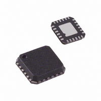
ADL5382ACPZ-R7 Analog Devices Inc, ADL5382ACPZ-R7 Datasheet - Page 24

ADL5382ACPZ-R7
Manufacturer Part Number
ADL5382ACPZ-R7
Description
IC DEMOD QUAD 700M2.7GHZ 24LFCSP
Manufacturer
Analog Devices Inc
Datasheet
1.ADL5382ACPZ-R7.pdf
(28 pages)
Specifications of ADL5382ACPZ-R7
Design Resources
Interfacing ADL5382 to AD9262 as an RF-to-Bits Solution (CN0062)
Function
Demodulator
Lo Frequency
700MHz ~ 2.7GHz
Rf Frequency
700MHz ~ 2.7GHz
P1db
14.5dBm
Gain
3.3dB
Noise Figure
17.6dB
Current - Supply
220mA
Voltage - Supply
4.75 V ~ 5.25 V
Package / Case
24-VFQFN, 24-CSP Exposed Pad
Frequency Range
700MHz To 2.7GHz
Rf Type
Quadrature
Supply Voltage Range
4.75V To 5.25V
Rf Ic Case Style
LFCSP
No. Of Pins
24
Operating Temperature Range
-40°C To +85°C
Lead Free Status / RoHS Status
Lead free / RoHS Compliant
Other names
ADL5382ACPZ-R7TR
Available stocks
Company
Part Number
Manufacturer
Quantity
Price
Company:
Part Number:
ADL5382ACPZ-R7
Manufacturer:
Analog Devices Inc
Quantity:
1 881
Part Number:
ADL5382ACPZ-R7
Manufacturer:
ADI/亚德诺
Quantity:
20 000
ADL5382
Table 4. Evaluation Board Configuration Options
Component
VPOS, GND
R1, R3, R6
C1, C2, C3,
C4, C8, C9
C6, C7,
C10, C11
R4, R5,
R9 to R16
L1, L2,
R7, R8
T2, T3
C12, C13
T4
T1
R2
Function
Power Supply and Ground Vector Pins.
Power Supply Decoupling. Shorts or power supply decoupling resistors.
These capacitors provide the required decoupling up to 2.7 GHz.
AC Coupling Capacitors. These capacitors provide the required ac coupling from
700 MHz to 2.7 GHz.
Single-Ended Baseband Output Path. This is the default configuration of the evaluation
board. R14 to R16 and R4, R5, and R13 are populated for appropriate balun interface.
R9, R10 and R11, R12 are not populated. Baseband outputs are taken from QHI and IHI.
The user can reconfigure the board to use full differential baseband outputs. R9 to R12
provide a means to bypass the 9:1 TCM9-1 transformer to allow for differential baseband
outputs. Access the differential baseband signals by populating R9 to R12 with 0 Ω and
not populating R4, R5, R13 to R16. This way the transformer does not need to be
removed. The baseband outputs are taken from the SMAs of Q_HI, Q_LO, I_HI, and I_LO.
Input Biasing. Inductance and resistance sets the input biasing of the common
base input stage. The default value is 33 nH.
IF Output Interface. TCM9-1 converts a differential high impedance IF output to a single-
ended output. When loaded with 50 Ω, this balun presents a 450 Ω load to the device.
The center tap can be decoupled through a capacitor to ground.
Decoupling Capacitors. C12 and C13 are the decoupling capacitors used to reject noise
on the center tap of the TCM9-1.
LO Input Interface. The LO is driven differentially. ETC1-1-13 is a 1:1 RF balun that
converts the single-ended RF input to differential signal.
RF Input Interface. ETC1-1-13 is a 1:1 RF balun that converts the single-ended RF input
to differential signal.
R
BIAS
. Optional bias setting resistor. See the Bias Circuit section to see how to use this feature.
Rev. 0 | Page 24 of 28
Default Condition
Not applicable
R1, R3, R6 = 0 Ω (0603)
C2, C4, C8 = 100 pF (0402)
C1, C3, C9 = 0.1 μF (0603)
C6, C10, C11 = 1000 pF (0402)
C7 = open
R4, R5, R13 to R16 = 0 Ω (0402)
R9 to R12 = open
L1, L2 = 33 nH (0603CS-33NX,
Coilcraft)
R7, R8 = 0 Ω (0402)
T2, T3 = TCM9-1, 9:1
(Mini-Circuits)
C12, C13 = 0.1 μF (0402)
T4 = ETC1-1-13, 1:1 (M/A-COM)
T1 = ETC1-1-13, 1:1 (M/A-COM)
R2 = open


