AT42QT1070-SSU Atmel, AT42QT1070-SSU Datasheet - Page 23
AT42QT1070-SSU
Manufacturer Part Number
AT42QT1070-SSU
Description
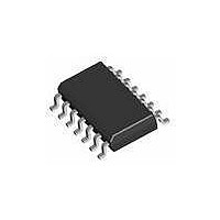
IC TOUCH SENSOR 7KEY 14-SOIC
Manufacturer
Atmel
Type
Capacitiver
Specifications of AT42QT1070-SSU
Number Of Inputs/keys
7 Key (Comms), 5 Key (Standalone)
Data Interface
I²C
Voltage Reference
Internal
Voltage - Supply
1.8 V ~ 5.5 V
Operating Temperature
-40°C ~ 85°C
Mounting Type
Surface Mount
Package / Case
14-SOIC (0.154", 3.90mm Width)
Supply Voltage
1.8 V to 5.5 V
Dimensions
3 mm L x 3 mm W x 0.8 mm H
Temperature Range
- 40 C to + 85 C
Termination Style
SMD/SMT
Lead Free Status / RoHS Status
Lead free / RoHS Compliant
Current - Supply
-
Resolution (bits)
-
Touch Panel Interface
-
Data Rate/sampling Rate (sps, Bps)
-
Lead Free Status / Rohs Status
Lead free / RoHS Compliant
Available stocks
Company
Part Number
Manufacturer
Quantity
Price
Company:

Part Number:
AT42QT1070-SSU
Manufacturer:
ATMEL
Quantity:
2 000
Company:
Part Number:
AT42QT1070-SSU QS529
Manufacturer:
Atmel
Quantity:
4 905


3.2.3
Touch Sensors Design Guide
Ground Loading
This style of sensor is highly sensitive to ground loading because such loading adds directly to Cx, thus
reducing the sensor’s gain. Any signal or power rail that runs under, or close to, the electrode will reduce
its gain. Note that ground in this context is anything that looks like an AC ground from the electrode’s
point of view and therefore encompasses just about any circuit element or feature that is nearby.
Note that traces from other sensing channels of the same chip can act as ground, depending on the
device.
Some QT devices only burst (acquire) a single channel at a time; when a channel is not bursting, it is
clamped to ground. Thus, two electrodes placed together that do not parallel burst will act as field
shapers against each other, since one will be at ground potential while the other acquires. If a trace
leading to key 1, say, is routed past key 2, then key 2 “sees” a ground trace next to it during its burst.
Other QT devices use “parallel bursts” where several keys burst at the same time; the signals on these
traces are at a similar potential during bursts, making them “self-shielding” and hence non-grounding
and non-interfering with respect to each other.
Electrodes when not acquiring are held at ground potential, and therefore act as a ground plane on
neighboring acquiring electrodes and diminish sensitivity overall, particularly at the edges. While these
effects can be overcome by increasing the value of Cs, it is still helpful to understand why these effects
happen, even if they cannot be improved due to panel design constraints.
Sometimes it is desirable to shield an electrode on its rear side to prevent false detection from moving
par ts to the rear, or to prevent interference from high voltage AC signals (such as from
electroluminescent backlighting or driver circuitry). Either an active shield with a solid metal plane behind
the electrodes or a rear ground plane can be used. If a ground plane is used, the ground should be
connected directly to the chip’s Vss pin to provide a clean ground having no relative voltage spikes on it.
Also, the electrode and ground plane should be separated by the maximum distance of air or thickness
of insulator possible.
Where a flood plane is absolutely required behind a sensor (perhaps to stop reverse side touch
sensitivity), and if the flood plane is on a layer that is a reasonable distance away (perhaps the back face
of a 1.6 mm FR4 PCB), then the trade-off between sensitivity loss and the desired operation may be
acceptable. In this case, always consider using a 50 percent mesh flood rather than a solid one, as this
will reduce the parasitic loading.
Electrodes will propagate fields into the panel material and laterally around the key area as well. These
fields will drop off gradually with distance from the edge of the key; sometimes this can result in key
detection some distance away from the key itself. It can therefore be beneficial to place hatched or solid
ground floods on the same layer as the electrodes, and near to the electrodes themselves, ideally
stopping the ground flood at about ½T away
further down in the stack, if this is more convenient, but the upper layer is preferred as it tends to offer
superior shielding.
1. It is acceptable to stop closer, but some loss of sensitivity will be observed. Experimentation will be required to
reach the best compromise.
(1)
(see
Figure
Self-capacitance Zero-dimensional Sensors
3-5). The ground flood can also be on layers
10620D–AT42–04/09
3-3
Related parts for AT42QT1070-SSU
Image
Part Number
Description
Manufacturer
Datasheet
Request
R

Part Number:
Description:
DEV KIT FOR AVR/AVR32
Manufacturer:
Atmel
Datasheet:

Part Number:
Description:
INTERVAL AND WIPE/WASH WIPER CONTROL IC WITH DELAY
Manufacturer:
ATMEL Corporation
Datasheet:
Part Number:
Description:
Low-Voltage Voice-Switched IC for Hands-Free Operation
Manufacturer:
ATMEL Corporation
Datasheet:
Part Number:
Description:
MONOLITHIC INTEGRATED FEATUREPHONE CIRCUIT
Manufacturer:
ATMEL Corporation
Datasheet:
Part Number:
Description:
AM-FM Receiver IC U4255BM-M
Manufacturer:
ATMEL Corporation
Datasheet:
Part Number:
Description:
Monolithic Integrated Feature Phone Circuit
Manufacturer:
ATMEL Corporation
Datasheet:
Part Number:
Description:
Multistandard Video-IF and Quasi Parallel Sound Processing
Manufacturer:
ATMEL Corporation
Datasheet:
Part Number:
Description:
High-performance EE PLD
Manufacturer:
ATMEL Corporation
Datasheet:
Part Number:
Description:
8-bit Flash Microcontroller
Manufacturer:
ATMEL Corporation
Datasheet:
Part Number:
Description:
2-Wire Serial EEPROM
Manufacturer:
ATMEL Corporation
Datasheet: