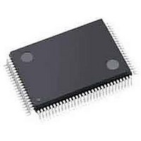
LFXP3C-3TN100I Lattice, LFXP3C-3TN100I Datasheet - Page 15

LFXP3C-3TN100I
Manufacturer Part Number
LFXP3C-3TN100I
Description
FPGA - Field Programmable Gate Array 3.1K LUTs 62 IO 1.8/ 2.5/3.3V -3 Spd I
Manufacturer
Lattice
Specifications of LFXP3C-3TN100I
Number Of Programmable I/os
62
Data Ram Size
55296
Supply Voltage (max)
3.465 V
Maximum Operating Temperature
+ 100 C
Minimum Operating Temperature
- 40 C
Mounting Style
SMD/SMT
Supply Voltage (min)
1.71 V
Package / Case
TQFP-100
Package
100TQFP
Family Name
LatticeXP
Device Logic Units
3000
Maximum Internal Frequency
320 MHz
Typical Operating Supply Voltage
1.8|2.5|3.3 V
Maximum Number Of User I/os
62
Ram Bits
55296
Re-programmability Support
Yes
Lead Free Status / RoHS Status
Lead free / RoHS Compliant
Available stocks
Company
Part Number
Manufacturer
Quantity
Price
Company:
Part Number:
LFXP3C-3TN100I
Manufacturer:
Lattice Semiconductor Corporation
Quantity:
10 000
Lattice Semiconductor
Table 2-6. sysMEM Block Configurations
Bus Size Matching
All of the multi-port memory modes support different widths on each of the ports. The RAM bits are mapped LSB
word 0 to MSB word 0, LSB word 1 to MSB word 1 and so on. Although the word size and number of words for
each port varies, this mapping scheme applies to each port.
RAM Initialization and ROM Operation
If desired, the contents of the RAM can be pre-loaded during device configuration. By preloading the RAM block
during the chip configuration cycle and disabling the write controls, the sysMEM block can also be utilized as a
ROM.
Memory Cascading
Larger and deeper blocks of RAMs can be created using EBR sysMEM Blocks. Typically, the Lattice design tools
cascade memory transparently, based on specific design inputs.
Single, Dual and Pseudo-Dual Port Modes
Figure 2-14 shows the four basic memory configurations and their input/output names. In all the sysMEM RAM
modes the input data and address for the ports are registered at the input of the memory array. The output data of
the memory is optionally registered at the output.
Single Port
True Dual Port
Pseudo Dual Port
Memory Mode
2-12
Configurations
8,192 x 1
4,096 x 2
2,048 x 4
1,024 x 9
256 x 36
8,192 x 1
4,096 x 2
2,048 x 4
1,024 x 9
512 x 18
8,192 x 1
4,096 x 2
2,048 x 4
1,024 x 9
512 x 18
256 x 36
512 x 18
LatticeXP Family Data Sheet
Architecture


