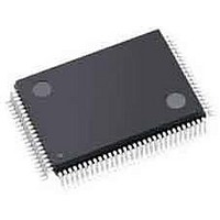
LFXP3C-3TN100I Lattice, LFXP3C-3TN100I Datasheet - Page 31

LFXP3C-3TN100I
Manufacturer Part Number
LFXP3C-3TN100I
Description
FPGA - Field Programmable Gate Array 3.1K LUTs 62 IO 1.8/ 2.5/3.3V -3 Spd I
Manufacturer
Lattice
Specifications of LFXP3C-3TN100I
Number Of Programmable I/os
62
Data Ram Size
55296
Supply Voltage (max)
3.465 V
Maximum Operating Temperature
+ 100 C
Minimum Operating Temperature
- 40 C
Mounting Style
SMD/SMT
Supply Voltage (min)
1.71 V
Package / Case
TQFP-100
Package
100TQFP
Family Name
LatticeXP
Device Logic Units
3000
Maximum Internal Frequency
320 MHz
Typical Operating Supply Voltage
1.8|2.5|3.3 V
Maximum Number Of User I/os
62
Ram Bits
55296
Re-programmability Support
Yes
Lead Free Status / RoHS Status
Lead free / RoHS Compliant
Available stocks
Company
Part Number
Manufacturer
Quantity
Price
Company:
Part Number:
LFXP3C-3TN100I
Manufacturer:
Lattice Semiconductor Corporation
Quantity:
10 000
Lattice Semiconductor
master serial clock is 2.5MHz. Table 2-10 lists all the available Master Serial Clock frequencies. When a different
Master Serial Clock is selected during the design process, the following sequence takes place:
1. User selects a different Master Serial Clock frequency for configuration.
2. During configuration the device starts with the default (2.5MHz) Master Serial Clock frequency.
3. The clock configuration settings are contained in the early configuration bit stream.
4. The Master Serial Clock frequency changes to the selected frequency once the clock configuration bits are
For further information on the use of this oscillator for configuration, please see details of additional technical docu-
mentation at the end of this data sheet.
Table 2-10. Selectable Master Serial Clock (CCLK) Frequencies During Configuration
Density Shifting
The LatticeXP family has been designed to ensure that different density devices in the same package have the
same pin-out. Furthermore, the architecture ensures a high success rate when performing design migration from
lower density parts to higher density parts. In many cases, it is also possible to shift a lower utilization design tar-
geted for a high-density device to a lower density device. However, the exact details of the final resource utilization
will impact the likely success in each case.
received.
1. Default
CCLK (MHz)
10.0
2.5
4.3
5.4
6.9
8.1
9.2
1
CCLK (MHz)
2-28
13
15
20
26
30
34
41
CCLK (MHz)
130
45
51
55
60
—
—
LatticeXP Family Data Sheet
Architecture


