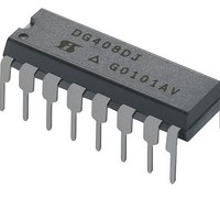
DG408LDY-E3 Vishay, DG408LDY-E3 Datasheet

DG408LDY-E3
Specifications of DG408LDY-E3
Related parts for DG408LDY-E3
DG408LDY-E3 Summary of contents
Page 1
... DG408/409. DG409L GND DG408L/409L Vishay Siliconix APPLICATIONS D Data Acquisition Systems D Battery Operated Equipment D Portable Test Equipment D Sample and Hold Circuits D Communication Systems D SDSL, DSLAM D Audio and Video Signal Routing , The DG409L Dual-In- Line, SOIC and TSSOP GND Decoders/Drivers ...
Page 2
... V consult “Digital Control” parameters for specific V+ operation. EN DG408L ORDERING INFORMATION Part Number Temp Range DG408LDY - 40 to 85_C 40 to 85_C DG408LDQ DG408LAK DG408LAK/883 - 55 to 125_C DG408LAZ/883 *Block Diagram and Pin Configuration not shown. Power Dissipation (Package) 16-Pin Plastic TSSOP 14 V 16-Pin Narrow SOIC ...
Page 3
... V (DG409L S1b S1b Room See Figure 3 Full = nF Room L GEN GEN Room f = 100 kHz 100 kHz Room MHz Room MHz 2 Room MHz 2 Room (DG409L only Room EN A DG408L/409L Vishay Siliconix A Suffix D Suffix - 55 to 125_C - 40 to 85_C Min Max Min Max Typ ...
Page 4
... DG408L/409L Vishay Siliconix SPECIFICATIONS (DUAL SUPPLY Parameter Symbol Analog Switch e Analog Signal Range V ANALOG Drain-Source On-Resistance r DS(on) I S(off Switch Off Leakage Current Switch Off Leakage Current I D(off) Channel On Leakage I D(on) a Current Digital Control Logic High Input Voltage V INH Logic Low Input Voltage ...
Page 5
... V (DG409L (DG409L S1b S1b Room See Figure 3 Full = nF Room L GEN GEN Room kW 100 kHz = 100 kHz L L Room MHz Room MHz Room MHz 2 Room (DG409L only) DG408L/409L Vishay Siliconix A Suffix D Suffix - 55 to 125_C - 40 to 85_C Min Max Min Max Typ 1 ...
Page 6
... DG408L/409L Vishay Siliconix SPECIFICATIONS (SINGLE SUPPLY 3 V) Parameter Symbol Analog Switch e Analog Signal Range V ANALOG Drain-Source On-Resistance r DS(on) I S(off Switch Off Leakage Current Switch Off Leakage Current I D(off) a Channel On Leakage Current I D(on) Digital Control Logic High Input Voltage V INH Logic Low Input Voltage ...
Page 7
... V - Drain Voltage (V) D Document Number: 71342 S-03720—Rev. D, 07-Apr- 85_C DG408L/409L Vishay Siliconix r vs. V and Power Supply DS(on Drain Voltage ( vs. V and Temperature DS(on) D 85_C 125_C 25_C - 55_C Drain Voltage (V) D Switching Time vs. Positive Supply Voltage t TRANS OFF 0 0 ...
Page 8
... DG408L/409L Vishay Siliconix TYPICAL CHARACTERISTICS (25_C UNLESS NOTED) Leakage Current vs. Analog Voltage S(off D(off) I D(on Analog Voltage ( Charge Injection vs. Analog Voltage 1 1000 0.6 0 0.2 0 Source Voltage (V) S Drain/Source Capacitance vs. Analog Voltage 35 C D(on D(off S(off www.vishay.com 110 Switching Time vs. ...
Page 9
... EN V- TEST CIRCUITS DG408L GND V- 300 DG409L GND V- 300 W V- Document Number: 71342 S-03720—Rev. D, 07-Apr-03 Level Decode/ Shift Drive FIGURE Logic O Input Switch Output SB4 FIGURE 2. Transition Time DG408L/409L Vishay Siliconix 50 90% 50% 90 TRANS (DG408L (DG409L) 4 www.vishay.com <20 ns < TRANS 9 ...
Page 10
... DG408L/409L Vishay Siliconix TEST CIRCUITS DG408L GND DG409L A 1 GND All S and DG408L A 1 DG409L GND www.vishay.com 300 300 FIGURE 3. Enable Switching Time bbm.5 4/9 Logic Input Switch Output 300 FIGURE 4. Break-Before-Make Interval 3 V Logic Input 50 ON(EN Switch Output V O 90% ...
Page 11
... Input Switch 1 nF Output V- V- FIGURE 5. Charge Injection OUT Channel Select GND V OUT V IN DG408L/409L Vishay Siliconix 3 V OFF the measured voltage due to charge transfer O error Q, when the channel turns off GND Crosstalk = 20 log FIGURE 7. Crosstalk Meter HP4192A S 8 Impedance Analyzer ...


