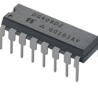
DG408LDY-E3 Vishay, DG408LDY-E3 Datasheet - Page 6

DG408LDY-E3
Manufacturer Part Number
DG408LDY-E3
Description
Multiplexer Switch ICs LV Single 8:1 3-bit Multiplexer/MUX
Manufacturer
Vishay
Type
Analog Multiplexerr
Specifications of DG408LDY-E3
Supply Current
0.2 mA
On Resistance (max)
80 Ohms
Propagation Delay Time
60 ns
On Time (max)
95 ns
Off Time (max)
100 ns
Supply Voltage (max)
12 V
Supply Voltage (min)
2.7 V
Maximum Power Dissipation
600 mW
Maximum Operating Temperature
+ 85 C
Minimum Operating Temperature
- 40 C
Package / Case
SOIC-16 Narrow
Mounting Style
SMD/SMT
Number Of Switches
Single
No. Of Circuits
1
On State Resistance Max
20ohm
Supply Voltage Range
3V To 6V
Operating Temperature Range
-40°C To +85°C
Analogue Switch Case Style
SOIC
No. Of Pins
16
Package
16SOIC N
Maximum On Resistance
80@2.7V Ohm
Maximum Propagation Delay Bus To Bus
60@12V|60@±5V|125@5V|150@3V ns
Maximum High Level Output Current
30 mA
Multiplexer Architecture
8:1
Maximum Turn-off Time
100@3V ns
Maximum Turn-on Time
95@3V ns
Power Supply Type
Single|Dual
Lead Free Status / RoHS Status
Lead free / RoHS Compliant
Lead Free Status / RoHS Status
Lead free / RoHS Compliant, Lead free / RoHS Compliant
DG408L/409L
Vishay Siliconix
Notes
a.
b.
c.
d.
e.
f.
g.
h.
i.
www.vishay.com
6
SPECIFICATIONS (SINGLE SUPPLY 3 V)
Analog Switch
Analog Signal Range
Drain-Source On-Resistance
Switch Off Leakage Current
Switch Off Leakage Current
Channel On Leakage Current
Digital Control
Logic High Input Voltage
Logic Low Input Voltage
Input Current
Dynamic Characteristics
Transition Time
Break-Before-Make Time
Enable Turn-On Time
Enable Turn-Off Time
Charge Injection
Off Isolation
Crosstalk
Source Off Capacitance
Drain Off Capacitance
Drain On Capacitance
Leakage parameters are guaranteed by worst case test condition and not subject to production test.
Room = 25_C, Full = as determined by the operating temperature suffix.
The algebraic convention whereby the most negative value is a minimum and the most positive a maximum, is used in this data sheet.
Typical values are for DESIGN AID ONLY, not guaranteed nor subject to production testing.
Guaranteed by design, not subject to production test.
V
Dr
Worst case isolation occurs on Channel 4 do to proximity to the drain pin.
r
DS(on)
IN
DS(on)
= input voltage to perform proper function.
Parameter
e
flatness is measured as the difference between the minimum and maximum measured values across a defined Analog signal.
e, h
= r
a
DS(on)
e
e
Max - r
e
e
e
a
a
DS(on)
a
Symbol
V
Min.
t
t
t
OFF(EN)
r
ANALOG
C
C
C
t
ON(EN)
X
I
TRANS
OIRR
DS(on)
I
I
V
OPEN
V
S(off)
D(off)
D(on)
TALK
S(off)
D(off)
D(on)
I
INH
Q
INL
IN
V+ = 2.7 V, V
V+ = 3 3 V V
V+ = 3.3 V, V
Unless Otherwise Specified
V
C
V
V
V
V
V
S1b
L
S(all)
AX
AX
f = 1 MHz, V
f = 1 MHz, V
S1
AX
f = 1 MHz, V
V+ = 3.3 V, V
= 1 nF, R
V+ = 3 V, "10%, V- = 0 V
Sequence Each Switch On
V
= 0 V V
= 0 V, V
= 1.5 V, V
= 1.5 V, V
AX
= 0 V, V
f = 100 kHz R
f = 100 kHz, R
Test Conditions
= V
V
EN
= V
DA
(DG409L only)
D
S
S
See Figure 2
See Figure 3
= 0.4 V or 2.0 V
EN
GEN
= 0.5 or 2.2 V, I
= 2 or 1 V V
= 2 or 1 V, V
S1b
S1b
S1
= 1.5 V, See Figure 4
S
D
D
S8
S4b
= 2.4 V or 0.4 V
D
= 1.5 V (DG408L)
= 0 V, V
= 0 V, V
= 0 V, V
= 1 5 V (DG409L)
= 1.5 V (DG409L)
= 0 W, V
= V
= 0 V, (DG408L)
= 0 V, (DG409L)
L
L
S
= 1 kW
= 1 kW
= 1 or 2 V
EN
EN
EN
D
D
GEN
f
= 1 or 2 V
= 1 or 2 V
= 0 V
= 0 V
= 2 V
S
= 0 V
= 5 mA
Temp
Room
Room
Room
Room
Room
Room
Room
Room
Room
Room
Room
Room
Room
Room
Full
Full
Full
Full
Full
Full
Full
Full
Full
Full
Full
Full
b
Typ
0.4
- 70
- 79
60
75
32
70
55
19
33
8
d
Min
- 1.5
- 55 to 125_C
- 15
- 15
- 15
- 1
- 1
- 1
A Suffix
0
2
1
c
Max
105
150
175
115
100
115
0.4
1.5
80
15
15
15
95
3
1
1
1
5
c
S-03720—Rev. D, 07-Apr-03
Document Number: 71342
Min
- 10
- 10
- 10
- 40 to 85_C
- 1
- 1
- 1
- 1
D Suffix
0
2
1
c
Max
100
150
175
105
100
105
0.4
80
10
10
10
95
3
1
1
1
1
5
c
Unit
nA
mA
pC
dB
dB
pF
pF
ns
ns
V
W
V
V


