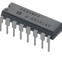
DG408LDY-E3 Vishay, DG408LDY-E3 Datasheet - Page 11

DG408LDY-E3
Manufacturer Part Number
DG408LDY-E3
Description
Multiplexer Switch ICs LV Single 8:1 3-bit Multiplexer/MUX
Manufacturer
Vishay
Type
Analog Multiplexerr
Specifications of DG408LDY-E3
Supply Current
0.2 mA
On Resistance (max)
80 Ohms
Propagation Delay Time
60 ns
On Time (max)
95 ns
Off Time (max)
100 ns
Supply Voltage (max)
12 V
Supply Voltage (min)
2.7 V
Maximum Power Dissipation
600 mW
Maximum Operating Temperature
+ 85 C
Minimum Operating Temperature
- 40 C
Package / Case
SOIC-16 Narrow
Mounting Style
SMD/SMT
Number Of Switches
Single
No. Of Circuits
1
On State Resistance Max
20ohm
Supply Voltage Range
3V To 6V
Operating Temperature Range
-40°C To +85°C
Analogue Switch Case Style
SOIC
No. Of Pins
16
Package
16SOIC N
Maximum On Resistance
80@2.7V Ohm
Maximum Propagation Delay Bus To Bus
60@12V|60@±5V|125@5V|150@3V ns
Maximum High Level Output Current
30 mA
Multiplexer Architecture
8:1
Maximum Turn-off Time
100@3V ns
Maximum Turn-on Time
95@3V ns
Power Supply Type
Single|Dual
Lead Free Status / RoHS Status
Lead free / RoHS Compliant
Lead Free Status / RoHS Status
Lead free / RoHS Compliant, Lead free / RoHS Compliant
TEST CIRCUITS
Vishay Siliconix maintains worldwide manufacturing capability. Products may be manufactured at one of several qualified locations. Reliability data for Silicon
Technology and Package Reliability represent a composite of all qualified locations. For related documents such as package/tape drawings, part marking, and
reliability data, see www.vishay.com/ppg?71342.
Document Number: 71342
S09-1259-Rev. F, 13-Jul-09
V
V
S
V
g
S
R
g
R
= 50
g
= 50
R
Ω
g
Ω
V
IN
Channel
Select
S
A
A
A
1
0
1
2
GND
S
S
A
A
A
X
8
0
1
2
Figure 8. Insertion Loss
GND
Figure 6. Off Isolation
EN
V+
V+
Insertion Loss = 20 log
EN
V+
V+
EN
S
A
A
A
X
0
1
2
GND
Off Isolation = 20 log
V-
V-
V-
V-
D
V+
V+
D
V-
V-
R
1
L
kΩ
R
1
D
V
L
kΩ
V
V
V
OUT
O
V
IN
OUT
V
IN
O
Figure 5. Charge Injection
C
1 nF
L
V
O
Channel
Select
R
g
= 50
Switch
Output
Logic
Input
Ω
V
S
A
A
A
3 V
0 V
GND
2
1
0
ΔV
error Q, when the channel turns off.
O
V
Figure 9. Source Drain Capacitance
IN
is the measured voltage due to charge transfer
OFF
EN
V+
V+
S
S
S
A
A
A
1
X
8
0
1
2
Figure 7. Crosstalk
DG408L, DG409L
GND
V-
V-
Q = C
S
S
D
1
8
ON
V+
V+
EN
L
Vishay Siliconix
Crosstalk = 20 log
x ΔV
O
V-
V-
D
www.vishay.com
or Equivalent
OFF
Impedance
HP4192A
f = 1 MHz
Analyzer
Meter
V
ΔV
R
1
V
OUT
L
IN
kΩ
O
V
O
11


