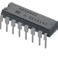
DG408LDY-E3 Vishay, DG408LDY-E3 Datasheet - Page 4

DG408LDY-E3
Manufacturer Part Number
DG408LDY-E3
Description
Multiplexer Switch ICs LV Single 8:1 3-bit Multiplexer/MUX
Manufacturer
Vishay
Type
Analog Multiplexerr
Specifications of DG408LDY-E3
Supply Current
0.2 mA
On Resistance (max)
80 Ohms
Propagation Delay Time
60 ns
On Time (max)
95 ns
Off Time (max)
100 ns
Supply Voltage (max)
12 V
Supply Voltage (min)
2.7 V
Maximum Power Dissipation
600 mW
Maximum Operating Temperature
+ 85 C
Minimum Operating Temperature
- 40 C
Package / Case
SOIC-16 Narrow
Mounting Style
SMD/SMT
Number Of Switches
Single
No. Of Circuits
1
On State Resistance Max
20ohm
Supply Voltage Range
3V To 6V
Operating Temperature Range
-40°C To +85°C
Analogue Switch Case Style
SOIC
No. Of Pins
16
Package
16SOIC N
Maximum On Resistance
80@2.7V Ohm
Maximum Propagation Delay Bus To Bus
60@12V|60@±5V|125@5V|150@3V ns
Maximum High Level Output Current
30 mA
Multiplexer Architecture
8:1
Maximum Turn-off Time
100@3V ns
Maximum Turn-on Time
95@3V ns
Power Supply Type
Single|Dual
Lead Free Status / RoHS Status
Lead free / RoHS Compliant
Lead Free Status / RoHS Status
Lead free / RoHS Compliant, Lead free / RoHS Compliant
DG408L, DG409L
Vishay Siliconix
Notes:
a. Leakage parameters are guaranteed by worst case test condition and not subject to production test.
b. Room = 25 °C, full = as determined by the operating temperature suffix.
c. The algebraic convention whereby the most negative value is a minimum and the most positive a maximum, is used in this datasheet.
d. Typical values are for DESIGN AID ONLY, not guaranteed nor subject to production testing.
e. Guaranteed by design, not subject to production test.
f. V
g. ΔR
h. Worst case isolation occurs on channel 4 do to proximity to the drain pin.
i. R
www.vishay.com
4
SPECIFICATIONS Dual Supply V+ = 5 V, V = 5 V
Parameter
Analog Switch
Analog Signal Range
Drain-Source
On-Resistance
Switch Off Leakage
Current
Channel On Leakage
Current
Digital Control
Logic High Input Voltage
Logic Low Input Voltage
Input Current
Dynamic Characteristics
Transition Time
Break-Before-Make
Time
Enable Turn-On Time
Enable Turn-Off Time
Source Off Capacitance
Drain Off Capacitance
Drain On Capacitance
IN
DS(on)
DS(on)
= input voltage to perform proper function.
e
a
a
flatness is measured as the difference between the minimum and maximum measured values across a defined analog signal.
= R
a
DS(on)
e
max. - R
e
e
e
e
e
e
V
DS(on)
Symbol
t
R
t
t
OFF(EN)
ANALOG
C
C
C
t
ON(EN)
TRANS
I
I
I
V
V
OPEN
DS(on)
S(off)
D(off)
D(on)
S(off)
D(off)
D(on)
I
INH
INL
IN
min.
V
V
V
V+ = 5 V, ± 10 %
EN
V
S1b
EN
V
S1
V
f = 1 MHz, V
AX
= 2.4 V, V
f = 1 MHz, V
f = 1 MHz, V
Unless Otherwise Specified
AX
= 0 V, V
= 3.5 V, V
= 3.5 V, V
Sequence Each Switch On
V
V
= 0 V, V
AX
= 0 V, V
D
V+ = 5.5 V, V- = - 5.5 V
V
V+ = 5.5 , V- = 5.5 V
V
=
= V
EN
S(all)
Test Conditions
±
D
See Figure 2
See Figure 4
See Figure 3
D
EN
= 0.6 V or 2.4 V
3.5 V, I
S1b
=
S1
S8
S4b
= V
D
=
D
S
= 2.4 V or 0.6 V
±
= 0 V, V
,
= 3.5 V (DG408L)
= - 3.5 V, (DG408L)
±
= 3.5 V (DG409L)
= 0 V, V
= 0 V, V
V- = - 5 V
= - 3.5 V, (DG409L)
DA
4.5 V, V
4.5 V, V
S
= 3.5 V
= 10 mA
EN
EN
EN
S
S
,
= 2.4 V
=
= 0 V
= 0 V
f
V- = 0 V
=
4.5 V
4.5 V
±
±
Temp.
Room
Room
Room
Room
Room
Room
Room
Room
Room
Room
Room
Full
Full
Full
Full
Full
Full
Full
Full
Full
Full
Full
Full
b
Typ.
20
30
25
20
15
29
8
6
d
- 55 °C to 125 °C
Min.
- 1.5
- 15
- 15
- 15
2.4
- 5
- 1
- 1
- 1
1
A Suffix
c
Max.
1.5
0.6
40
50
15
15
15
60
78
55
68
40
50
5
1
1
1
S09-1259-Rev. F, 13-Jul-09
c
Document Number: 71342
- 40 °C to 85 °C
Min.
- 10
- 10
- 10
2.4
- 5
- 1
- 1
- 1
- 1
1
D Suffix
c
Max.
0.6
40
50
10
10
10
60
65
55
60
40
45
5
1
1
1
1
c
Unit
nA
µA
pF
ns
Ω
V
V


