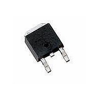
BUK663R5-30C,118 NXP Semiconductors, BUK663R5-30C,118 Datasheet - Page 3

BUK663R5-30C,118
Manufacturer Part Number
BUK663R5-30C,118
Description
MOSFET N-CH TRENCH D2PACK
Manufacturer
NXP Semiconductors
Series
TrenchMOS™r
Datasheet
1.BUK663R5-30C118.pdf
(14 pages)
Specifications of BUK663R5-30C,118
Input Capacitance (ciss) @ Vds
4707pF @ 25V
Fet Type
MOSFET N-Channel, Metal Oxide
Fet Feature
Standard
Rds On (max) @ Id, Vgs
3.5 mOhm @ 25A, 10V
Drain To Source Voltage (vdss)
30V
Current - Continuous Drain (id) @ 25° C
100A
Vgs(th) (max) @ Id
2.8V @ 1mA
Gate Charge (qg) @ Vgs
78nC @ 10V
Power - Max
158W
Mounting Type
Surface Mount
Package / Case
TO-263-3, D²Pak (2 leads + Tab), TO-263AB
Configuration
Single
Transistor Polarity
N-Channel
Resistance Drain-source Rds (on)
3.5 mOhms
Drain-source Breakdown Voltage
30 V
Gate-source Breakdown Voltage
+/- 20 V
Continuous Drain Current
100 A
Power Dissipation
158 W
Maximum Operating Temperature
+ 175 C
Mounting Style
SMD/SMT
Minimum Operating Temperature
- 55 C
Lead Free Status / RoHS Status
Lead free by exemption / RoHS compliant by exemption
NXP Semiconductors
4. Limiting values
Table 4.
In accordance with the Absolute Maximum Rating System (IEC 60134).
[1]
[2]
[3]
[4]
[5]
[6]
BUK663R5-30C
Product data sheet
Symbol
V
V
I
I
P
T
T
Source-drain diode
I
I
Avalanche ruggedness
E
E
D
DM
S
SM
stg
j
DS
GS
tot
DS(AL)S
DS(AL)R
-16V accumulated duration not to exceed 168 hrs.
Accumulated pulse duration not to exceed 5mins.
Continuous current is limited by package.
Single-pulse avalanche rating limited by maximum junction temperature of 175 °C.
Repetitive avalanche rating limited by an average junction temperature of 170 °C.
Refer to application note AN10273 for further information.
Limiting values
Parameter
drain-source voltage
gate-source voltage
drain current
peak drain current
total power dissipation
storage temperature
junction temperature
source current
peak source current
non-repetitive drain-source
avalanche energy
repetitive drain-source
avalanche energy
All information provided in this document is subject to legal disclaimers.
Rev. 02 — 16 November 2010
Conditions
T
DC
Pulsed
T
T
T
see
T
T
t
I
V
p
D
j
mb
mb
mb
mb
mb
GS
≤ 10 µs; pulsed; T
≥ 25 °C; T
= 100 A; V
Figure 3
= 25 °C; V
= 100 °C; V
= 25 °C; t
= 25 °C; see
= 25 °C
= 10 V; T
j
sup
≤ 175 °C
j(init)
p
GS
≤ 10 µs; pulsed;
GS
≤ 30 V; R
Figure 2
= 10 V; see
= 25 °C; unclamped
= 10 V; see
N-channel TrenchMOS intermediate level FET
mb
= 25 °C
GS
= 50 Ω;
Figure 1
Figure 1
BUK663R5-30C
[1]
[2]
[3]
[3]
[3]
[4][5][6]
Min
-
-16
-20
-
-
-
-
-55
-55
-
-
-
-
© NXP B.V. 2010. All rights reserved.
175
175
Max
30
16
20
100
100
616
158
100
616
242
-
Unit
V
V
V
A
A
A
W
°C
°C
A
A
mJ
J
3 of 14


